 Professional Flip-Chip Packaging Substrate Supplier

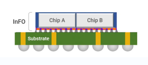
What are 2D IC Package Substrates?
2D IC Package Substrate manufacturer and 2D IC Package Service . the Package Substrate will be made with Showa Denko and Ajinomoto High speed materials or other types base materials.
2D IC Package Substrates are an important part of PCB engineering and they play a key role in integrated circuit packaging. These substrates provide a flat surface that supports and connects semiconductor devices, providing necessary support for the functionality and performance of electronic systems.
In PCB engineering, 2D IC Package Substrates are used as the basis for IC packages. They carry one or more integrated circuit chips and provide electrical connections and thermal management. These substrates are often made from different types of materials, including organic materials, ceramics, metal cores and flexible materials, to meet the needs of various applications.
2D IC Package Substrates are closely related to integrated circuit packaging. They package the chip on the substrate and use metalized connecting wires to connect the chip to other components. This packaging and connection process ensures a stable and reliable connection between the chip and the external system, while providing the necessary thermal conduction and mechanical support.
In summary, 2D IC Package Substrates are key elements in PCB engineering, providing support and connections for integrated circuit packaging while ensuring the performance and reliability of electronic systems.
What types of 2D IC Package Substrates are there?
2D IC Package Substrates are an important part of PCB engineering and come in many types, each with its own unique characteristics and applications. The following are some common types:
Organic substrate is one of the most common types, usually using fiberglass reinforced resin (FR-4) as the substrate. They have the characteristics of low cost, easy processing and good insulation properties. Organic substrates are suitable for many standard applications and are the first choice for many electronic products.
Ceramic substrates have excellent thermal conductivity and mechanical strength, making them widely used in high-power and high-frequency applications. They can effectively dissipate heat and have good dimensional stability and signal integrity, making them suitable for scenarios that require high stability and reliability.
The metal core base has a metal core layer that conducts heat efficiently. This makes them excellent for thermal management in compact electronic devices. Metal core substrates are suitable for applications requiring high thermal conductivity such as LED lighting, power modules and automotive electronics.
Flexible substrates are flexible and lightweight, so they can bend and twist, making them suitable for the design of flexible electronics. They play an important role in areas such as wearable devices, flexible circuit boards, and curved displays.
Each type of 2D IC Package Substrates has unique advantages and applicability, allowing engineers to select the most appropriate type based on specific application needs to achieve optimal performance and reliability.
What are the advantages of 2D IC Package Substrates?
2D IC Package Substrates are highly favored in modern PCB engineering, not only because they have a series of unique advantages over other types of boards, but also because they can bring significant improvements to the performance and reliability of electronic systems.
First, 2D IC Package Substrates have higher integration and functionality than traditional PCB boards. By integrating multiple components and functional units on a single substrate, 2D IC Package Substrates enable more compact designs, saving space and increasing the performance density of the system. This highly integrated design can also reduce the number of connection points in the circuit and reduce signal transmission paths, thereby reducing signal transmission delay and improving system response speed.
Second, 2D IC Package Substrates excel in thermal management. Because they are typically made from materials with good thermal conductivity properties, such as ceramic or metal substrates, they are able to conduct and disperse heat efficiently. This is especially important for high-power applications or compact electronic devices to prevent chip damage due to overheating and ensure long-term stable operation of the system.
In addition, 2D IC Package Substrates have excellent electrical properties. By using advanced manufacturing processes and materials, these substrates enable low-loss signal transmission and stable signal integrity, ensuring circuit reliability and stability. This is critical for high-frequency, high-speed, or high-precision applications such as communications equipment, computer servers, and medical instrumentation.
In addition, 2D IC Package Substrates offer good reliability and durability. Because they use high-quality materials and strict manufacturing processes, they are able to maintain stable performance in various harsh environments and have a long service life. This makes them ideal for many critical applications, such as aerospace, medical and military, where equipment reliability and stability are extremely important.
In summary, 2D IC Package Substrates are favored because they have significant advantages in integration, thermal management, electrical performance, reliability and durability, and can provide solutions for the design and manufacturing of electronic systems. Provide superior solutions.
Why choose 2D IC Package Substrates?
In modern PCB engineering, 2D IC Package Substrates are gradually becoming the first choice instead of traditional PCB boards. This is no accident, but rather because 2D IC Package Substrates bring a series of significant advantages that make them uniquely valuable in electronic packaging.
2D IC Package Substrates provide excellent thermal management capabilities, which are critical to the stability and performance of electronic devices. They dissipate heat more efficiently than traditional PCB boards, keeping devices operating within safe temperature ranges, thereby extending the life of electronic equipment.
2D IC Package Substrates offer superior electrical performance due to shorter signal transmission paths and lower signal losses. This enables electronic systems to achieve higher speeds and lower power consumption, thereby improving overall system performance.
The design of 2D IC Package Substrates is more compact and can accommodate more devices and connection lines, thereby achieving a higher level of integration. Compared with traditional PCB boards, they can achieve smaller and lighter designs and are suitable for applications with high space requirements.
2D IC Package Substrates offer higher reliability and durability due to the use of advanced materials and manufacturing processes. They are able to withstand harsher environmental conditions while reducing the risk of failure due to material aging or thermal stress, thereby increasing system stability and reliability.
Although 2D IC Package Substrates may be slightly more expensive than traditional PCBs in some aspects, they often achieve better cost-effectiveness in the long run given the superior performance and reliability they offer. In addition, with the advancement of technology and market competition, the price of 2D IC Package Substrates is gradually declining, further enhancing its competitiveness in the market.
In summary, compared to traditional PCB boards, choosing 2D IC Package Substrates has many advantages, including excellent thermal management capabilities, enhanced electrical performance, compact design and high integration, improved reliability and durability, and good cost-effectiveness. These advantages make 2D IC Package Substrates an indispensable and important component in today’s electronic engineering field, bringing more reliable and advanced solutions to the design and manufacturing of electronic devices.
How to manufacture 2D IC Package Substrates?
2D IC Package Substrates (two-dimensional integrated circuit packaging substrates) are a key component in modern circuit board engineering. Their manufacturing process involves multiple key steps to ensure their high performance and reliability in electronic packaging.
The manufacturing of 2D IC Package Substrates begins with the preliminary preparation phase, which includes the preparation and preparation of raw materials. The key to this step is to ensure that the selected substrate meets the requirements of the specific application, such as an organic substrate, a ceramic substrate, or a metal core substrate.
The next critical step in the manufacturing process is layer stacking. This involves stacking different layers of substrates together in a precise manner to form the basic structure of 2D IC Package Substrates. The order and manner in which the layers are layered has a profound impact on the performance and functionality of the final product.
In the manufacturing of 2D IC Package Substrates, details and special layers are added by using advanced techniques, including processes such as photolithography, etching, and chemical deposition. These layers may include metal wires, insulation, and other necessary structures to ensure the stability and performance of the circuit.
Using photolithography, manufacturers precisely define circuit patterns on 2D IC Package Substrates. This step determines the board layout, connections, and component locations and is a critical link in the entire manufacturing process.
In the final stages of 2D IC Package Substrates manufacturing, pads and connection components are added to the circuit board. This ensures a strong connection of the electronic components, allowing the board to interact effectively with other electronic components.
Surface treatment is the final step in the manufacturing process whereby 2D IC Package Substrates are given final surface coatings and treatments to improve their corrosion resistance and durability. This helps ensure stable operation of the board in a variety of environmental conditions.
Through this series of key steps, manufacturers can produce 2D IC Package Substrates that are high-performance, reliable, and meet application-specific needs. This advanced manufacturing process enables electronic devices to play a greater role in different industries, thereby driving continuous innovation in electronic engineering.
What are the application areas of 2D IC Package Substrates?
2D IC Package Substrates are a key electronic packaging material with wide applications in multiple industries. Below we will explore in which areas we can see the application of 2D IC Package Substrates and their role in different industries.
In the field of consumer electronics, 2D IC Package Substrates are widely used in smartphones, tablets, smart watches and other portable devices. Their compact design and high performance enable these devices to achieve higher functional density and better performance. In addition, the thermal management properties of 2D IC Package Substrates help keep the temperature of the device stable, ensuring its reliability over long periods of operation.
In the field of automotive electronics, 2D IC Package Substrates are widely used in automotive electronic control units (ECUs), driving assistance systems, entertainment systems and vehicle communication equipment. Their high reliability and vibration resistance allow them to adapt to the various harsh environments in which cars are driven, while providing stable performance.
In the aerospace field, 2D IC Package Substrates are used in avionics, navigation systems, communications equipment and satellite technology. Their lightweight design and high-performance characteristics make them ideal for the aerospace industry, where they can meet space constraints and high reliability requirements.
In the field of medical equipment, 2D IC Package Substrates are widely used in medical diagnostic equipment, medical monitoring equipment and medical imaging equipment. Their high performance and reliability enable medical equipment to provide accurate data and stable operation, thereby ensuring patient safety and the accuracy of medical diagnosis.
Overall, 2D IC Package Substrates play an important role in various industries, and their high performance, reliability, and versatility make them a key component of modern electronic devices. With the continuous advancement of technology and the continuous expansion of application fields, it is foreseeable that they will play an even more important role in the future.
2D IC Package Substrate
Where can I find 2D IC Package Substrates?
What is the best way to find 2D IC Package Substrates? In terms of finding suppliers with reliable quality, our company provides the following suggestions and methods.
Internet search: Through search engines, such as Google or Baidu, enter the keyword “2D IC Package Substrates supplier” or “2D IC Package Substrates manufacturer” to obtain a large amount of relevant information. Browse the supplier’s website to learn about its product range, quality certifications, production capabilities, and customer feedback.
Industry exhibitions: Attending relevant electronics industry exhibitions or exhibitions is another effective way to find 2D IC Package Substrates suppliers. These shows bring together numerous electronic component manufacturers and suppliers, providing you with the opportunity to directly contact and learn about their products.
Online platform: Through online electronic component trading platforms, such as Alibaba, Global Sources or eBay, you can browse to 2D IC Package Substrates suppliers around the world. These platforms usually provide supplier details, product catalogs, prices and transaction terms to facilitate your comparison and selection.
Refer to recommendations from industry insiders: Ask peers, industry experts, or electronic engineers who work in the electronics industry for their recommendations and suggestions. Their experience and insights may provide you with valuable references in finding quality and reliable 2D IC Package Substrates suppliers.
Our company’s supplier network: Our company has established a solid supplier network, including a number of suppliers with rich experience and good reputation in the field of 2D IC Package Substrates. By contacting our company, we can provide relevant supplier information and provide you with customized solutions to meet your needs and requirements.
When selecting a supplier, in addition to focusing on product quality and price, factors such as the supplier’s delivery capability, after-sales service, and history of cooperation with the supplier should also be considered. Through comprehensive consideration, you can find the 2D IC Package Substrates supplier that best suits your needs and provide reliable support for your project.
What is the quote for 2D IC Package Substrates?
When getting a quote for 2D IC Package Substrates, key factors include material type, size, quantity, customization requirements, and the supplier’s pricing strategy. How to evaluate these factors and get an accurate quote is discussed below.
First, the cost of purchasing 2D IC Package Substrates depends on the type of material selected. Generally, organic-based materials (such as FR-4) are relatively cheap, while ceramic-based materials are more expensive due to their excellent thermal conductivity and reliability. Additionally, metal-based materials vary in cost, depending on the type and quality of the metal core.
Secondly, size and quantity are two other important factors that affect cost. Larger sized 2D IC Package Substrates typically require more material and processing costs and are therefore more expensive. At the same time, discounts are usually available for bulk purchases, so the price of mass-produced 2D IC Package Substrates is relatively lower.
Customization requirements also have an impact on costs. If special processes or design customization are required, this may increase manufacturing costs. However, some suppliers may offer customized services and adjust prices based on customer demand.
Finally, methods to obtain relevant quotes include contacting suppliers directly, making inquiries through online platforms or e-commerce websites, and attending industry exhibitions to negotiate with suppliers. Contacting the supplier directly is probably the most direct and quick method as they can provide a personalized quote based on your specific needs. At the same time, prices and services from different suppliers can be easily compared through online platforms or e-commerce websites. Participating in industry exhibitions can not only learn about the latest technologies and trends, but also communicate face-to-face with suppliers and obtain more detailed quotation information.
To summarize, the cost of purchasing 2D IC Package Substrates depends on several factors, including material type, size, quantity, customization requirements, and the supplier’s pricing strategy. By carefully evaluating these factors and taking the appropriate approach to obtaining quotes can help you obtain an accurate and reasonable price and select the 2D IC Package Substrates that best suit your needs.
Frequently Asked Questions (FAQs)
What are 2D IC Package Substrates?
2D IC Package Substrates are foundational layers used in integrated circuit (IC) packaging. They provide a platform for mounting and interconnecting semiconductor chips within electronic systems.
What types of 2D IC Package Substrates are available?
There are several types of 2D IC Package Substrates, including organic substrates, ceramic substrates, metal core substrates, and flex substrates. Each type offers unique characteristics suited for different applications.
What advantages do 2D IC Package Substrates offer?
2D IC Package Substrates offer advantages such as enhanced thermal management, improved electrical performance, miniaturization capabilities, higher reliability, and cost-effectiveness compared to traditional PCBs.
Why choose 2D IC Package Substrates over other boards?
2D IC Package Substrates provide superior thermal management, electrical performance, and miniaturization capabilities, making them ideal for modern electronic designs requiring high reliability and performance.
How are 2D IC Package Substrates manufactured?
The manufacturing process of 2D IC Package Substrates involves substrate preparation, layer buildup, interconnection, and surface finishing using advanced techniques such as lithography, etching, and plating.
What are the applications of 2D IC Package Substrates?
2D IC Package Substrates find applications across various industries, including consumer electronics, automotive, aerospace, medical devices, and telecommunications, powering a wide range of electronic systems and devices.
Where can I find 2D IC Package Substrates?
Reputable suppliers and manufacturers offer a diverse range of 2D IC Package Substrates, catering to custom and standard requirements. Online marketplaces and industry-specific trade shows are valuable resources for procuring high-quality substrates.