 Professional Flip-Chip Packaging Substrate Supplier

What are CSP Package Substrates?
CSP Package Substratemanufacture. we can produce the best samllest bump pitch with 100um, the best smallest trace are 9um.
CSP Package Substrates, or chip-scale packaging substrates, are an advanced packaging solution that plays a key role in modern PCB (Printed Circuit Board) engineering. In the PCB design and manufacturing process, selecting the appropriate packaging method is crucial, and CSP Package Substrates are favored for their unique design and performance advantages.
In traditional package design, the package is typically much larger than the integrated circuit chip itself. This means more space is needed around the chip to accommodate the package. CSP Package Substrates uses a package that is almost the same size as the chip, so its size is much smaller than traditional packages, which allows electronic devices to be designed more compactly. They are typically lighter and thinner than traditional packages, making them ideal for applications with stringent weight and volume requirements, such as portable electronics and smart wearables.
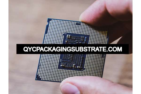
CSP Package Substrate
In modern PCB engineering, CSP Package Substrates play a key role. They provide flexibility and efficiency in the design and manufacture of electronic devices. Due to their compact size, a higher level of component integration can be achieved, thereby increasing board performance and reliability. In addition, they can reduce the length of signal transmission on the circuit board, thereby reducing signal delay and loss and improving the overall performance of the circuit board.
CSP Package Substrates also provide PCB engineers with greater design freedom. They enable higher density wiring, allowing designers to achieve more functionality in a limited space. At the same time, they can also simplify design and reduce manufacturing costs by reducing the hierarchical structure of the circuit board.
Overall, CSP Package Substrates play an integral role in modern PCB engineering. They have revolutionized the manufacturing and application of electronic devices through their compact size, high performance, and flexible design. Whether in the fields of consumer electronics, automotive electronics, medical equipment or communication equipment, CSP Package Substrates has demonstrated its irreplaceable advantages and value.
What types of CSP Package Substrates are there?
In modern PCB engineering, CSP (Chip Scale Package) Package Substrates have become a key packaging solution due to their miniaturization and high performance. We’ll dive into the various types of CSP Package Substrates and their unique features.
Organic CSP Package Substrates utilize an organic substrate, typically fiberglass-reinforced epoxy. Features of this type include:
Lightweight design: Due to the lightweight nature of organic materials, the overall package is lighter and suitable for lightweight electronic devices.
Relatively low manufacturing costs: Organic substrates are easy to process during the manufacturing process, so the manufacturing costs are relatively low.
Ceramic CSP Package Substrates use ceramic substrates with the following features:
Excellent thermal conductivity: Ceramic materials have good thermal conductivity, which helps to effectively dissipate heat and is suitable for high-performance electronic equipment.
Corrosion resistance: Ceramics are highly resistant to chemical substances, improving the stability of electronic components.
Metal Core CSP Package Substrates have substrates with integrated metal layers that provide unique properties:
Excellent heat dissipation performance: The metal core substrate can effectively conduct and dissipate heat, making it suitable for high-power applications.
Structural Strength: The metal core substrate provides additional structural strength, making it suitable for applications with high physical stress.
Flexible CSP Package Substrates use flexible substrates with the following unique features:
Flexible design: The flexible base material allows CSP to adapt to curves and special-shaped designs, improving design flexibility.
Thin and short: The thin and thin nature of flexible substrates makes CSP advantageous in lightweight and portable devices.
Each type of CSP Package Substrates has its unique advantages in different application scenarios, and design engineers can choose the most appropriate type based on project needs to achieve optimal performance and reliability. This diversity allows CSP Package Substrates to meet different market needs while also promoting continuous innovation in electronic packaging technology.
What are the advantages of using CSP Package Substrates?
In modern PCB engineering, CSP (Chip Scale Package) Package Substrates play an important role and bring many unique advantages. Below we’ll explore the motivations for choosing CSP Package Substrates and their advantages over other boards.
A significant advantage of CSP Package Substrates is their size. Compared with traditional packaging solutions, CSP is smaller and almost the same size as the chip. This compact design allows the board to be more compact, saving space, which is crucial especially for small and portable devices.
CSP Package Substrates excel in thermal management. Due to the smaller package size, its thermal conduction path is shorter, helping to effectively disperse and remove heat. This is critical for thermal management in high-performance devices and applications, ensuring that electronic components remain within the appropriate temperature range while operating.
Compared with traditional PCB packaging solutions, CSP Package Substrates also have improved electrical performance. Due to the smaller package size, the connection length is shorter, which reduces the delay and loss of signal transmission. This is especially important for high-frequency applications and scenarios that require fast data transmission.
CSP Package Substrates are designed to improve overall system reliability. Smaller package size means tighter connections between components, reducing the impact of the external environment on connections. Additionally, due to its smaller size, CSP is also more resistant to mechanical stress and vibration, thereby increasing the system’s vibration resistance and durability.
Although the initial investment may be slightly higher, given the many advantages of CSP Package Substrates, they are often a more cost-effective option over the long term. The size advantage means material cost savings in the design, and its superior thermal management and electrical performance characteristics also reduce system operating costs.
In summary, CSP Package Substrates have been widely used in modern PCB engineering due to their size advantages, thermal management capabilities, improved electrical performance, enhanced reliability and cost-effectiveness. For electronic equipment manufacturers pursuing high performance, miniaturization and reliability, choosing CSP Package Substrates is a wise choice that can bring greater competitive advantages to their products.
Why choose CSP Package Substrates?
In today’s rapidly evolving electronics industry, choosing the right packaging solution is crucial. CSP Package Substrates (chip-scale packaging substrates) are getting a lot of attention in this area because they offer unique advantages over traditional packaging solutions.
First, one of the biggest advantages of CSP Package Substrates is their compact size. Compared with traditional packaging, the size of the CSP package is almost the same as the integrated circuit chip itself, allowing the overall size of the electronic device to be significantly reduced. This compact design makes CSP Package Substrates particularly suitable for space-critical applications such as smartphones, wearables, and IoT devices.
Secondly, CSP Package Substrates also have excellent electrical properties. Due to the smaller package size, CSP Package Substrates can reduce electrical connection lengths, thereby reducing signal delays and losses. This advantage makes CSP Package Substrates excellent in high-frequency and high-speed data transmission applications, helping to improve the overall performance and stability of the device.
Additionally, CSP Package Substrates offer excellent thermal performance. Despite its smaller size, heat can be transferred to the surrounding environment more efficiently due to the direct contact between the CSP package and the chip. This makes CSP Package Substrates ideal for applications with high thermal management requirements, such as high-performance computing and industrial control systems.
In addition, CSP Package Substrates provide greater reliability. Due to the small package size, CSP packages are more robust than traditional packages and are more resistant to mechanical stress and vibration. This gives CSP Package Substrates a longer life and less vulnerability to damage in a variety of harsh environments.
Overall, CSP Package Substrates have become the preferred packaging solution in modern electronic device design due to their compact size, excellent electrical performance, excellent thermal performance and high reliability. As technology continues to advance and market demands continue to change, CSP Package Substrates will continue to play an important role and will play an increasingly important role in the future electronics industry.
What is the manufacturing process for CSP Package Substrates?
The manufacturing process of CSP Package Substrates is a complex and precise process involving multiple critical steps to ensure the quality and performance of the final product. The following are the general steps of the manufacturing process for CSP Package Substrates:
The first step in the manufacturing process is to prepare the substrate. Typically, the substrate is made of organic materials (such as fiberglass-reinforced epoxy) or ceramic materials. These substrates require rigorous cleaning and surface treatment to ensure accuracy and reliability in subsequent process steps.
Next, CSP Package Substrates are built by stacking different material layers. These layers may include conductive layers, insulating layers, copper foil layers, etc. Each layer must be precisely placed and aligned according to design requirements.
After the layer stacking is completed, the chips and other components are assembled onto the substrate. This may involve soldering, gluing or other connection methods to ensure a good connection between the component and the substrate.
Once the components are assembled, metallization takes place. This process involves depositing a metal layer, usually copper or nickel, on the surface of a substrate. The purpose of metallization is to provide conductivity and provide preparation for subsequent component connection and packaging.
Finally, CSP Package Substrates are surface treated to enhance their performance and durability. This may include chemical treatments, matte finishes, or metal plating. The surface treatment helps protect the substrate from the environment and provides better connectivity and reliability.
Strict quality control and inspection procedures are crucial throughout the entire manufacturing process. By using advanced technology and equipment, as well as strict process controls, manufacturers can ensure the production of high-quality, reliable performance CSP Package Substrates.
Overall, the manufacturing processes for CSP Package Substrates require a high degree of technical expertise and precision craftsmanship, but they provide critical performance advantages and manufacturing flexibility for electronic devices.
What are the application areas of CSP Package Substrates?
CSP Package Substrates are advanced packaging solutions that are widely used in various industries. Their high performance and compact design make them useful in many fields.
In the field of consumer electronics, CSP Package Substrates are one of the core components of devices such as smartphones, tablets, and wearable devices. Since these devices have very stringent size and performance requirements, the small size and superior electrical performance of CSP Package Substrates make them the first choice. In addition, in the design of consumer electronics products, CSP Package Substrates also provide higher reliability and better thermal management, thereby extending the life of the device.
In the automotive industry, CSP Package Substrates play a key role in advanced driver assistance systems (ADAS) and in-vehicle infotainment systems. These systems place extremely high demands on the size and performance of electronic components, and CSP Package Substrates are able to meet these requirements while providing reliable performance and durability to handle the harsh conditions of the automotive operating environment.
In the aerospace and defense sector, CSP Package Substrates are used to manufacture a variety of avionics and satellite communications systems. Their high-density packaging and reliability make them ideal for spacecraft and military equipment, capable of operating in extreme environments and maintaining stability.
The medical industry is also one of the important application areas for CSP Package Substrates. These packaging solutions are used to manufacture a variety of medical devices, including implantable medical devices and diagnostic equipment. The miniaturization and high performance of CSP Package Substrates make medical devices more portable and flexible while maintaining a high level of functionality and reliability.
In the telecommunications sector, CSP Package Substrates are used to manufacture high-speed data transmission and networking equipment. These devices have extremely high requirements for size and performance, and CSP Package Substrates can meet these requirements and provide support for the stable operation of telecommunications networks.
To summarize, CSP Package Substrates play an important role in various industries, from consumer electronics to aerospace to medical and telecommunications, providing critical support and solutions for the design and manufacturing of devices.
Where can I find CSP Package Substrates?
Want to get high-quality CSP Package Substrates, you may ask: “Where can I find CSP Package Substrates?” The answer is at your fingertips. As a professional supplier, we offer you the best quality CSP Package Substrates to suit your project needs.
There are many supply channels for CSP Package Substrates in the market, but finding a reliable supplier is crucial. At our company, we offer you state-of-the-art CSP Package Substrates with high quality, reliability and professional services as our core philosophy.
Our company is known for its excellent reputation in the industry as a professional CSP Package Substrates supplier. We not only have advanced production equipment and technology, but also an experienced team, committed to providing customers with the highest quality products and services. Our CSP Package Substrates undergo rigorous quality control and testing to ensure their performance and reliability meet industry standards.
No matter the size of your project, we can provide you with a customized solution and ensure you get a product that matches your expectations exactly. Our customer service team is here to support you and ensure your purchasing process goes smoothly.
When choosing a supplier for CSP Package Substrates, remember to choose an experienced and reputable company to ensure your project runs smoothly and is a success. We look forward to working with you and providing you with quality CSP Package Substrates to help you achieve your project goals.
If you have any needs or questions about CSP Package Substrates, please feel free to contact our team and we will be happy to serve you.
What are the quotes for CSP Package Substrates?
Obtaining a quote for CSP Package Substrates is a critical step that involves multiple factors and requires careful consideration to ensure you receive an accurate and reasonable quote. Here are some important considerations about how to get a quote and what factors influence it:
First, to get a quote for CSP Package Substrates, it’s best to contact the supplier or manufacturer directly. These suppliers often offer online quoting tools or can be contacted by email or phone. By communicating directly with suppliers, you can receive more detailed and personalized quote information to meet your specific needs.
Quotes are affected by a variety of factors, including but not limited to the following:
Material Cost: The cost of CSP Package Substrates is affected by the cost of materials. Different types of materials (e.g. organic materials, ceramic materials, etc.) as well as the quality and supply scarcity of the materials all have an impact on costs.
Manufacturing Process: The manufacturing process of CSP Package Substrates may involve complex processes and technologies, including lamination, metallization, surface treatment, etc. The complexity and precision requirements of the manufacturing process directly impact costs.
Custom Requirements: If you have special custom requirements, such as specific dimensions, materials, or special workmanship requirements, then these custom requirements may result in additional costs.
Quantity and lot size: The purchase quantity also has a great influence on the quotation. Typically, larger discounts are available for larger quantities, while prices may be slightly higher for smaller quantities.
Delivery time: If you require expedited delivery or have specific delivery time requirements, this may have an impact on the quote. Typically, expedited service comes with additional costs.
All that said, to get an accurate quote for CSP Package Substrates, it’s best to contact the supplier directly and provide as much detail as possible, including your specific needs, customization requirements, and expected delivery time. Additionally, be aware of the impact of different factors on your quote so you can make sound budgets and decisions.
Frequently Asked Questions FAQS
Are CSP Package Substrates compatible with standard components?
Yes, CSP Package Substrates are designed to be compatible with standard components commonly used in electronic devices. Their compact size and efficient design make them suitable for integrating with various components, ensuring seamless compatibility.
What environmental considerations should be taken into account when using CSP Package Substrates?
When using CSP Package Substrates, it’s essential to consider factors such as temperature, humidity, and exposure to chemicals or contaminants. These substrates may have specific operating temperature ranges and environmental ratings, so it’s crucial to adhere to manufacturer guidelines for optimal performance and reliability.
How long do CSP Package Substrates typically last in operational environments?
The longevity of CSP Package Substrates in operational environments depends on various factors, including operating conditions, usage patterns, and quality of materials and manufacturing processes. Generally, when used within specified parameters and under appropriate environmental conditions, CSP substrates can have a long service life comparable to other packaging solutions.
Can CSP Package Substrates be customized for specific applications?
Yes, CSP Package Substrates can be customized to meet specific application requirements. Manufacturers often offer options for customization in terms of substrate materials, dimensions, layer configurations, and surface finishes. Customization allows designers to tailor CSP substrates to the unique needs of their projects, optimizing performance and functionality.
What are the primary challenges associated with using CSP Package Substrates?
While CSP Package Substrates offer numerous benefits, they also present challenges such as higher complexity in manufacturing processes, tighter design constraints due to miniaturization, and potential reliability issues related to solder joint integrity. However, these challenges can be effectively addressed through advanced technologies, robust quality control measures, and careful design considerations.