 Professional Flip-Chip Packaging Substrate Supplier

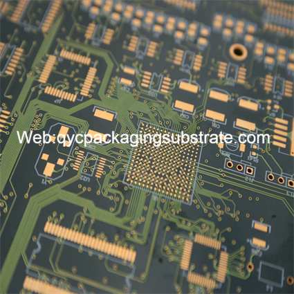
What is High speed materials substrate?
High speed substrate manufacture. we offer High speed PCB and High speed substrate from 2 layer to 50 layers. the best smallest bump pitch are 100um, the best smallest trace&gap are 9um/9um, commonly 15-30um design.
These materials boast low dielectric constants and low loss factors, enhancing the speed and quality of signal transmission. This characteristic aids in reducing signal distortion during the processing of high-frequency signals, ensuring a stable and reliable signal.
Furthermore, the design of high-speed material substrates prioritizes the optimization of signal integrity. Through meticulous planning of the substrate’s hierarchical structure, employing specific stacking methods, and implementing effective electromagnetic shielding measures, these substrates minimize signal reflection, crosstalk, and distortion during transmission. This meticulous design ensures high-quality signal transmission within the circuit.
Beyond their applications in high-frequency communications, high-speed material substrates find extensive use in radio frequency (RF), microwave, and millimeter-wave fields. These applications span critical areas such as 5G communications, radar systems, and satellite communications, where the ability to process high-frequency signals and facilitate fast data transmission is paramount.
Their special properties and material selection give them unique advantages in high-speed circuit design. Compared with conventional substrates, high-speed material substrates pay more attention to the control of signal speed, waveform and delay, and are suitable for various high-performance applications.
Overall, high-speed material substrates are one of the key factors driving the continued advancement of electronic technology. Its application in the fields of high-speed communications, radio frequency and microwave provides more reliable and efficient solutions for modern electronic equipment and promotes the development of the digital era.
What makes high-speed material substrates so unique?
Among them, High-Speed Materials Substrate, as a substrate material widely used in high-frequency electronic devices, is becoming increasingly unique and important. So, what makes high-speed material substrates so unique, let’s dig a little deeper.
High-speed material substrates possess unique qualities that make them well-suited for managing high-speed signals and data transmission. Primarily, the materials chosen for these substrates, often incorporating special dielectric materials like PTFE, are meticulously selected. These materials exhibit exceptional dielectric properties, effectively minimizing signal transmission losses and ensuring high-quality signal transmission.
Furthermore, the surface characteristics of high-speed material substrates are carefully crafted to uphold signal integrity. Precision processing of the surface is common, facilitating excellent impedance matching while reducing signal reflection and crosstalk. This precision is crucial in maintaining clear and stable signals, especially at high frequencies.
Additionally, high-speed material substrates exhibit outstanding thermal stability and mechanical strength, enabling them to remain stable in environments characterized by high temperatures and frequencies. This quality renders them highly applicable in high-performance electronic devices, particularly within the domains of communications, radar, and high-performance computing.
When selecting a high-speed material substrate, engineers also focus on its chemical resistance to ensure reliability under a variety of environmental conditions. This makes high-speed material substrates highly prized not only in high-frequency electronic devices, but also in applications in extreme environments.
What is the function of high-speed material substrate?
In today’s electronic field, the rise of high-speed circuits is a trend that cannot be ignored. In this field, what role does High-Speed Materials Substrate, as a key element, play?
By in-depth analysis of the key characteristics of high-speed material substrates, we can more fully understand its specific functions in circuit design. This includes optimization of signal integrity, transmission speed and interference immunity, providing strong support for the performance of electronic devices.
First, one of the key characteristics of high-speed material substrates is their excellent signal integrity. This substrate material is designed to operate in high-frequency environments, effectively reducing distortion during signal transmission. Its low loss and low dispersion characteristics enable it to maintain signal stability and ensure accurate signal transmission in the circuit.
Secondly, high-speed material substrates are crucial to the optimization of transmission speed. In modern electronic devices, data transmission speed is a crucial indicator. The superior electrical properties of high-speed material substrates enable them to support higher transmission speeds to meet growing data demands. This provides greater bandwidth for a variety of high-performance applications and drives technology development.
In addition, the high-speed material substrate also exhibits excellent anti-interference performance. In complex electromagnetic environments, equipment is often subject to various interferences. The high-speed material substrate effectively reduces the impact of external signals on the circuit through its outstanding anti-interference properties, ensuring that the equipment can operate stably under various working conditions.
Overall, high-speed material substrates are not only supporters of electronic devices, but also a key factor in promoting innovation in high-speed circuit design. Its superior performance in signal integrity, transmission speed and anti-interference has laid a solid foundation for the continuous progress of modern electronic technology. Therefore, we have a deep understanding of the functions of high-speed material substrates and can better apply it in circuit design to bring better performance and reliability to our electronic devices.
What are the different types of high-speed material substrates?
In the pursuit of high-speed circuits, particular attention is directed towards high-speed material substrates, given their distinctive properties. A comprehensive examination of various high-speed material substrates, such as PTFE substrates and mixed-k substrates, is essential to understand their respective advantages and limitations across diverse applications.
Critical to the design of high-speed electronic devices is the judicious selection of materials, where polytetrafluoroethylene (PTFE) substrates emerge prominently. Renowned for their exceptional dielectric properties, PTFE substrates boast low signal loss, optimal signal integrity, and superior high-frequency performance. These attributes make them a preferred choice in RF and microwave applications, raising the question of whether they are an ideal fit for your high-speed circuit designs.
However, in complex scenarios of high-speed circuit design, hybrid dielectric constant substrates also show their unique advantages. By properly mixing dielectric constants, this type of substrate can balance transmission speed and signal integrity in different frequency bands. Have we looked at how hybrid-k substrates perform in data transmission and high-frequency applications?
Has thorough exploration been conducted to understand their suitability for different application scenarios and their potential impact on circuit performance?
In summary, the landscape of high-speed material substrates is diverse, with each type possessing unique characteristics and tailored application areas. By delving into the specifics of materials like PTFE substrates and mixed dielectric constant substrates, we can make more informed choices for specific design requirements. This not only optimizes signal transmission performance but also presents a more adaptable and dependable option for high-speed circuit design. Thoughtful selection among different types of high-speed material substrates expands the horizons for future developments in high-speed electronic devices.
High speed materials substrate
What is the relationship between high-speed material substrates and IC packaging?
In the wave of high-speed electronic technology, have we previously had an in-depth understanding of the different types of high-speed material substrates, such as PTFE substrates and mixed dielectric constant substrates, and compared their characteristics in various applications? Now, we will further explore the close connection between high-speed material substrates and IC packaging.
The increasing popularity of high-speed electronic devices has made the relationship between high-speed material substrates and IC packaging critical. The synergy between high-speed material substrates as the basis of circuits and IC packaging is critical to ensuring signal integrity and performance.
The evolution of IC packaging and high-speed material substrates
First, let us review the evolution of IC packaging technology. As chip integration increases, the demand for faster signal transmission and heat dissipation is also increasing. At this time, high-speed material substrates entered the stage. They not only provided good signal transmission characteristics, but also effectively dealt with electrothermal issues and provided support for the stable operation of ICs.
The role of high-speed material substrates in IC packaging
High-speed material substrates play a key role in IC packaging. Its excellent dielectric properties enable signals to be transmitted more stably and quickly on the substrate, reducing the risk of signal distortion. At the same time, the superior thermal conductivity of high-speed material substrates helps maintain the temperature of the IC within a safe range and avoid the negative impact of overheating on device performance.
Applicability of different types of high-speed material substrates
Considering different types of high-speed material substrates, such as PTFE substrates and mixed dielectric constant substrates, each of them has unique applications in IC packaging. PTFE substrate is often used in scenarios that require extremely high signal transmission quality due to its low dielectric loss and stable dielectric properties. Hybrid dielectric constant substrates are excellent at balancing performance and cost and are suitable for some cost-sensitive applications.
What is the difference between high-speed material substrate and traditional PCB?
With the rapid development of the electronic field, the demand for high-speed circuits is growing day by day. This article will make an in-depth comparison between High Speed Materials Substrate and traditional PCB, PWB, motherboard and other related concepts, and explore its innovation and superiority in design.
High-speed material substrate is a substrate material widely used in high-frequency electronic equipment and has excellent high-speed signal processing capabilities. Have we compared high-speed material substrates with traditional concepts such as traditional PCBs, PWBs, and motherboards in detail to reveal their unique design features?
Comparison of high-speed material substrates and traditional PCBs
Compared with traditional PCBs, the key advantage of high-speed material substrates lies in material selection and processing. The use of high-speed materials such as PTFE substrate makes data transmission in high-frequency environments more efficient. Have we examined the properties of these materials and how they are superior to traditional PCB materials?
Innovative design of high-speed material substrates
Explore the innovation in design of high-speed material substrates, especially in terms of signal integrity and transmission speed. Does its superiority play a key role in high-speed data transmission in electronic devices?
Limitations of PWB and other traditional concepts
For PWB and other traditional concepts, have we analyzed their limitations in handling high-speed data transmission? Are innovations such as high-density interconnect (HDI) technology making high-speed material substrates a more reliable choice?
Changes in motherboard design
Traditional motherboards face limitations in high-speed circuit design due to factors such as signal integrity, crosstalk, and loss. The pursuit of faster data transfer rates and improved signal quality has led to a revolution in motherboard design, with a notable shift towards high-speed material substrates.
In contrast to traditional PCBs, high-speed material substrates are gaining popularity among design engineers for meeting the escalating demands of high-frequency applications. Understanding the differences between these substrates is crucial in comprehending why they are increasingly preferred in today’s electronic devices.
The main structures and production technologies of high-speed material substrates play a pivotal role in their application. The rapid evolution of electronic technology has elevated high-speed material substrates to a key status in circuit design. To grasp their importance in PCB engineering, it is essential to delve into the intricacies of their structure and manufacturing technology.
The distinctive structure of high-speed material substrates is fundamental to their superior performance in high-frequency electronic devices. These substrates typically feature a multi-layer design that incorporates high-frequency materials like PTFE (polytetrafluoroethylene), ensuring exceptional electrical performance. An essential aspect of their structure involves isolating different layers with fine dielectric layers, effectively reducing crosstalk and signal loss during transmission. This nuanced design contributes significantly to their effectiveness in high-frequency applications.
In structural design, how we skillfully apply high-density interconnect (HDI) technology is crucial. HDI technology greatly improves the integration of components on the board and the signal transmission efficiency by achieving a tighter component layout on the same layer and realizing interconnections between layers through fine apertures. This structural design provides a shorter path for high-speed signals and reduces the time delay of signal transmission, thereby meeting today’s challenges in data transmission speed requirements.
The manufacturing technology of high-speed material substrates is another key factor in ensuring their performance. In this regard, semi-additive manufacturing technology plays a huge role. Semi-Additive manufacturing technology adds copper layer by layer on the surface of the substrate, and then precisely defines the circuit pattern through photolithography and etching processes, allowing high-density and fine circuits to be realized. The application of this manufacturing technology provides higher production accuracy and more complex circuit design capabilities for high-speed material substrates.
In addition, improved high-density interconnect (HDI) technology also plays a key role in the manufacturing process. The introduction of HDI technology makes the interconnection between different layers more flexible, which not only increases the line density, but also enhances the reliability and stability of the circuit board. The continuous innovation of this technology has injected new vitality into the manufacturing of high-speed material substrates and adapted to the needs of increasingly complex electronic devices.
Throughout the entire manufacturing process, how we cleverly combine these key technologies to produce high-performance, high-reliability high-speed material substrates is a goal that engineers need to constantly pursue. Through the synergy of these technologies, we are better able to meet the critical performance, stability and reliability demands of today’s high-speed circuit designs.
Through in-depth analysis of high-speed material substrate structures and manufacturing technologies, we can better understand their role in electronic engineering and more flexibly apply these technologies in practical applications, laying a solid foundation for future electronic device design.
Frequently Asked Questions (FAQs)
In the process of discussing high-speed material substrates, we have provided in-depth answers to some common questions that readers may ask to help better understand the applications and advantages of high-speed material substrates.
How do high-speed material substrates improve signal integrity?
We explain in detail how signal integrity can be optimized in the design of high-speed material substrates to ensure the reliability and stability of high-frequency signal transmission.
What are the similarities and differences between different types of high-speed material substrates?
We compare different types of high-speed material substrates, including PTFE substrates and mixed-k substrates, to help readers choose the material that best suits their application needs.
What are the advantages of high-speed material substrates compared with traditional PCBs?
We discussed the innovation of high-speed material substrates compared to traditional PCBs, especially their superior performance in handling high-speed signals and data transmission.
What is special about the production technology of high-speed material substrates?
We gain an in-depth understanding of the manufacturing process of high-speed material substrates, including the application of improved high-density interconnect (HDI) technology and semi-additive manufacturing technology.
How to maximize the advantages of high-speed material substrates in practical applications?
We provide practical suggestions on how to make full use of the advantages of high-speed material substrates in actual circuit design to meet the needs of different application scenarios.
By answering these questions, we hope readers can gain a more comprehensive understanding of high-speed material substrates and better apply this technology in practice to promote innovation in the electronics field.