 Professional Flip-Chip Packaging Substrate Supplier

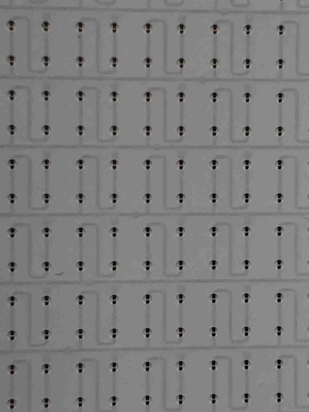
Microtrace/Gap LED PCB
Microtrace/Gap LED PCB Manufacturing. Ultra-small gap LED PCB has produced with Msap technology. we can produce 30um~70um gap mini LED PCBs.
Ultra-small gap substrates (ultra-small gap substrates) represent an innovative technology in today’s electronic engineering field and are specially designed to cope with the increasingly urgent size and performance requirements of modern electronic devices. This substrate has significant design features in terms of tiny gaps between electronic components, aiming to optimize their layout and performance.
This special design mainly includes the layout of ultra-small gaps, aiming to achieve higher integration and superior electrical performance. Typically, Ultra-small gap substrates minimize the gaps between electronic components through precise engineering design to achieve a more compact size layout. The purpose of this design is mainly to overcome the space limitations of traditional PCBs and provide more usable space for modern electronic devices, thereby achieving more powerful performance and functionality.
In this design, tiny gaps between electronic components play a key role. The existence of these tiny gaps allows the circuit board to accommodate more components, allowing electronic devices to achieve higher integration within a limited space. In addition, this tiny gap design helps reduce the signal transmission path in the circuit, thereby reducing transmission delay and improving signal transmission efficiency, providing a feasible solution to the requirements of high-performance electronic equipment.
The design goals of ultra-small gap substrates are not only limited to improving integration, but also include superior electrical performance and thermal management. Through tiny gaps, Ultra-small gap substrates can more effectively manage the heat generated by electronic devices, improve heat dissipation, and ensure that devices can maintain a stable operating temperature during high-performance operation, thereby extending device life and improving overall performance.
Innovation in the realm of electronic devices is epitomized by ultra-small gap substrates, meticulously designed to address the size and performance requisites of contemporary electronics. Characterized by its distinctive design, these substrates empower electronic engineers to attain heightened integration, superior electrical performance, and more efficient thermal management within constrained spaces. This unique design serves as a crucial foundation, offering essential support for the ongoing development and innovation in electronic equipment. Anticipated to continually evolve, this technology is poised to propel the field of electronic engineering to unprecedented heights.
What are the functions of Ultra-small gap substrates?
As an important innovation in the field of contemporary electronic engineering, Ultra-small gap substrates have many compelling functions. First, its design focuses on creating tiny gaps between electronic components, which provides the possibility to achieve highly integrated circuits.
In terms of achieving high integration, Ultra-small gap substrates adopt advanced design concepts and manufacturing technologies. Through precise inter-layer connections, the substrate accommodates more electronic components in a limited space, effectively improving the integration of the circuit. This not only makes the overall size of the device smaller, but also creates room for performance improvements in modern electronic products.
In terms of electrical performance, Ultra-small gap substrates achieve excellent electrical signal transmission performance through extremely small gap design.
At the same time, Ultra-small gap substrates also show unique advantages in thermal management. The tiny gap design helps improve thermal conductivity and effectively reduces the operating temperature of electronic components. This has a positive impact on stabilizing device performance and extending component life, especially in electronic products with high-density layouts.
The allure of ultra-small gap substrates has propelled them to popularity within the contemporary landscape of electronic engineering. Their application not only aligns with the imperative to consistently shrink the dimensions of electronic devices but also presents an innovative remedy for elevating circuit performance and refining thermal management. As technology progresses unabated, ultra-small gap substrates are poised to emerge as a crucial catalyst in electronic engineering design, steering the trajectory of electronic devices towards a future characterized by compactness, robustness, and heightened efficiency.
What are the different types of Ultra-small gap substrates?
Ultra-small gap substrates, as a key electronic component, play a vital role in meeting the needs of modern electronic devices for small size and high performance. To better understand this field, let’s dive into the different types of Ultra-small gap substrates, how they are classified, and how they differ in practical applications.
The different types of Ultra-small gap substrates are mainly classified based on their material composition and manufacturing process. From a material perspective, they can include organic substrates, glass substrates, etc. These different material types affect the physical properties and performance of Ultra-small gap substrates.
On the other hand, from a manufacturing process perspective, the manufacturing of Ultra-small gap substrates usually includes traditional PCB processes and some innovative manufacturing technologies. Traditional PCB processes may include steps such as printing, etching, and copper pouring, while innovative manufacturing technologies may involve more precise processes, such as Improved HDI manufacturing technology and Improved semi-additive methods. These differences in manufacturing processes directly affect the preparation accuracy, production efficiency and cost of Ultra-small gap substrates.
In applications, these different types of Ultra-small gap substrates play unique roles. The flexibility of organic substrates makes them more suitable for certain electronic devices that require curved designs, such as portable electronics. The mechanical strength of glass substrates may make them more suitable for applications that require higher stability and durability, such as industrial automation equipment.
Overall, the different types of Ultra-small gap substrates provide electronic engineers with more choices to meet the needs of different application scenarios. Understanding the characteristics and advantages of these types can help engineers make more informed choices during the design phase, thereby driving the electronics industry in a more innovative and efficient direction.
What is the relationship between Ultra-small gap substrates and IC packaging?
In today’s rapidly developing electronics field, Ultra-small gap substrates play a vital role in IC packaging. Its unique design and characteristics make it a key component in achieving high-performance chip packaging.
First, we need to understand the role of Ultra-small gap substrates in IC packaging. The design of this ultra-small gap substrate makes it possible to accommodate more electronic components in a limited space. This is critical for modern electronic devices, which often require smaller sizes and higher levels of integration. Ultra-small gap substrates provide technical support for the miniaturization and light weighting of electronic devices by providing smaller gaps and making chip packaging more compact.
In order to better understand the application of Ultra-small gap substrates in high-performance chip packaging, we can classify them by different chip packaging technologies. One common classification is based on differences in manufacturing processes. Improved HDI manufacturing technology and Improved semi-additive method are two representative technologies that play a key role in realizing high-performance chip packaging of Ultra-small gap substrates.
Improved HDI manufacturing technology enables a more compact circuit layout by using more refined manufacturing processes, including high-density wiring and micro-aperture holes. The application of this technology makes Ultra-small gap substrates more suitable to meet the requirements of modern electronic equipment for high integration and high transmission efficiency.
On the other hand, the Improved semi-additive method reduces the gaps between components by adding circuit components layer by layer on the surface of the substrate. This approach enables Ultra-small gap substrates to accommodate more components in a limited space and improve overall performance.
Overall, the role of Ultra-small gap substrates in IC packaging is not only reflected in their compact design, but also in their ability to achieve high-performance chip packaging through different manufacturing technologies. The application of this substrate not only meets the needs of modern electronic equipment for miniaturization and lightweight, but also provides key support for technological innovation and development in the electronic field. By in-depth understanding of the application of Ultra-small gap substrates in IC packaging, we can better grasp the development direction of the field of electronic engineering and meet future technical challenges.
Microtrace/Gap LED PCB,(White core and White soldermask)
What is the difference between Ultra-small gap substrates and common PCBs?
Ultra-small gap substrates, as one of the key technologies in the field of contemporary electronic engineering, show significant differences from traditional PCBs in terms of structure and manufacturing technology. Before we dive into these differences, let’s review the main types of traditional PCBs, including PWBs, Motherboard, Substrate-like PCB, and HDI substrate.
PWBs (Printed Wiring Boards) are the most basic circuit boards and are commonly used in simple electronic devices. Motherboard is the core board in the computer system and is responsible for connecting various components. Substrate-like PCB (SLP) and HDI substrate (High-Density Interconnect) are advanced circuit boards designed to meet high-density and high-performance requirements.
Compared with these traditional PCBs, Ultra-small gap substrates present unique characteristics in structure and manufacturing technology. First, they are designed to achieve extremely small component clearances to accommodate more electronic components in a limited space. This characteristic gives Ultra-small gap substrates significant advantages in high integration.
From a structural point of view, Ultra-small gap substrates have a more compact component layout and smaller gaps, so they can accommodate more functional units in the same size. This is different from the traditional PCB design concept, which pays more attention to the distance and stability between components.
In terms of manufacturing technology, Ultra-small gap substrates adopt a series of innovative methods, including Improved HDI manufacturing technology and Improved semi-additive method. The introduction of these technologies aims to improve the density and performance of circuit boards, making Ultra-small gap substrates capable of more complex electronic device designs.
On the other hand, traditional PCBs tend to use traditional processes in the manufacturing process. Compared with Ultra-small gap substrates, their manufacturing processes are relatively traditional. This makes Ultra-small gap substrates more suitable for electronic products requiring higher integration and smaller size.
Overall, the significant differences in structure and manufacturing technology of Ultra-small gap substrates make them ideal for meeting the urgent needs for high performance and small size in modern electronic devices. Through continuous innovation and the introduction of advanced technologies, Ultra-small gap substrates are expected to lead the development trend in the field of electronic engineering and promote the emergence of smaller and more powerful electronic devices.
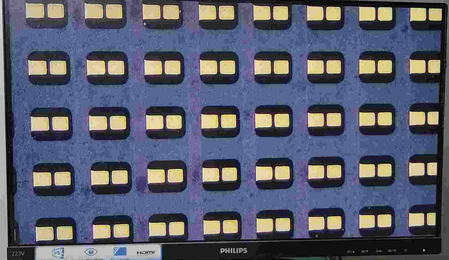
Ultra-small Trace/Spacing LED PCB , (Black core and Black soldermask)
What are the main structures and manufacturing technologies of Ultra-small gap substrates?
Ultra-small gap substrates are a technology that has attracted much attention in electronic engineering. Its major breakthroughs in design and manufacturing technology provide key support for the miniaturization and high performance of modern electronic devices.
Main structural design of Ultra-small gap substrates
Ultra-small gap substrates are designed to achieve the smallest gaps between electronic components, allowing more components to be accommodated in a limited space and achieving higher levels of integration. The key structural design of this substrate includes:
Minimal gap design: This design features electronic components
Multi-layer structure: Ultra-small gap substrates usually adopt a multi-layer structure to achieve more complex circuit layouts by stacking layers. This design allows circuits to be arranged in a vertical direction, further improving space utilization efficiency.
Advanced materials: In structural design, Ultra-small gap substrates use a series of advanced materials with excellent electrical conductivity, insulation and thermal conductivity properties to ensure the normal operation of electronic components and effectively manage the heat generated.
Manufacturing technology for Ultra-small gap substrates
The manufacturing of Ultra-small gap substrates involves a series of advanced technologies, including:
Improved HDI manufacturing technology: High-density insertion (HDI) technology is an important part of the manufacturing of Ultra-small gap substrates. Improved HDI manufacturing technology makes it possible to achieve more circuit connections in a limited space by using smaller apertures and higher inter-layer connection density.
Improved semi-additive method: Using the Improved semi-additive method, metal is only added to the required areas during the manufacturing process instead of traditional full coverage. This approach reduces material waste, improves manufacturing efficiency, and makes the production of Ultra-small gap substrates more precise and controllable.
Through these advanced manufacturing technologies, Ultra-small gap substrates not only innovate in structural design, but also achieve high precision and efficiency in the manufacturing process. The successful application of these technologies provides electronic engineers with more flexible options to cope with changing and improving technical requirements.
In essence, ultra-small gap substrates play a pivotal role in advancing the miniaturization and high performance of electronic devices, thanks to their distinctive structural design and cutting-edge manufacturing technology. Their extensive integration into electronic engineering not only fuels the evolution of a new generation of electronic equipment but also propels the ongoing advancement of science and technology.
What are the frequently asked questions about Ultra-small gap substrates?
Delving into the diverse applications and distinctive properties of ultra-small gap substrates, it becomes imperative to address frequently asked questions that orbit this innovative technology. Unveiling the answers to these inquiries is paramount in equipping readers with a comprehensive understanding of the capabilities inherent in this cutting-edge technological landscape.
How are Ultra-small gap substrates different from traditional PCBs?
Compared with traditional Printed Circuit Boards (PCBs), Ultra-small gap substrates have significant differences in structure and manufacturing technology. This issue involves the unique design of Ultra-small gap substrates and their advantages over traditional PCBs in terms of high integration and superior performance.
Why are Ultra-small gap substrates needed in electronic devices?
Understanding the necessity of Ultra-small gap substrates is critical to understanding their critical role in modern electronic devices. This issue will explore the rapid advancement and shrinking size of electronic devices and how Ultra-small gap substrates can meet this need.
What are the advantages of Ultra-small gap substrates in thermal management?
Thermal management has always been an important issue in the field of electronic engineering. Readers may wonder how Ultra-small gap substrates provide advantages in the heat dissipation of electronic components through their design.
What are the innovations in the manufacturing technology of Ultra-small gap substrates?
This issue will delve into the manufacturing technologies for Ultra-small gap substrates, including Improved HDI manufacturing technology and Improved semi-additive methods, and how these technologies support the realization of their unique properties.
What are the special applications of Ultra-small gap substrates in IC packaging?
IC packaging is a key step in the protection of electronic components. Readers may be concerned about how Ultra-small gap substrates are used in this field and how they are related to chip packaging technology.
How do Ultra-small gap substrates meet the demand for small size and high performance in electronic devices?
This question will lead readers to think deeply about how Ultra-small gap substrates meet the needs of modern electronic devices for small size and high performance through their unique design and performance advantages.
By answering these frequently asked questions, we can help readers gain a more comprehensive understanding of Ultra-small gap substrates, thereby better grasping knowledge in this field and its critical role in driving innovation and development in electronic engineering.