 Professional Flip-Chip Packaging Substrate Supplier

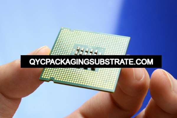
What is QFN Package?
QFN Package Manufacturer.High speed and high frequency material packaging substrate manufacturing. Advanced packaging substrate production and AFN package service.
QFN Package, Quad Flat No-Lead, is an integrated circuit package that has attracted much attention in the field of PCB engineering. The unique design of the QFN Package provides electronic designers with more flexibility and performance advantages compared to traditional packages. Let’s take a closer look at the secrets of this leadless package.
One of the features of the QFN Package is its low profile, leadless design. This design allows for a flat thermal pad on the bottom of the package without the need for external leads to connect the chip. This not only simplifies the appearance of the package, but also provides a larger soldering area, helping to improve soldering quality and reliability.
Another distinguishing feature of the QFN Package is its compact form factor. Since no external leads are required, the overall size of the QFN Package can be significantly reduced, making it ideal in space-constrained applications. Whether in consumer electronics or industrial equipment, QFN Package provides designers with greater design freedom and flexibility.
In addition, QFN Package also has excellent heat dissipation performance. The flat thermal pad on the bottom of the package not only directly contacts the heat sink or PCB board, but also effectively transfers heat, thereby improving the heat dissipation efficiency of the chip. This makes QFN Package particularly suitable for high-power applications or scenarios with high heat dissipation requirements.
QFN Package
In general, QFN Package, as a modern integrated circuit package, combines many advantages such as flatness, no leads, and excellent heat dissipation performance. Its emergence has opened up a new design space for electronic designers, allowing them to respond to different design challenges more flexibly.
What are the types of QFN Package substrates?
In the world of QFN Package substrates, organic, ceramic and metal substrates are the main types. These different types of substrates have their own unique characteristics and are suitable for different application needs.
First, organic substrates are an affordable and lightweight option. Due to their relatively low material costs, organic substrates are often widely used in cost-sensitive projects. Additionally, their lightness makes them very practical in designs where light weight is required.
Second, ceramic substrates are known for their excellent thermal conductivity and reliability. Ceramic materials have excellent thermal conductivity, which makes ceramic substrates excellent in applications that require efficient heat dissipation. In addition, ceramic substrates also have high mechanical strength and stability, making them suitable for applications that require high reliability.
Finally, metal substrates are favored for their excellent thermal management capabilities, especially for high-power applications. Metal substrates generally have high thermal conductivity and can effectively transfer heat from electronic devices to the external environment. This makes metal substrates ideal for applications requiring strong thermal dissipation performance.
In general, there are various types of QFN Package substrates, each type has its unique advantages and applicable scenarios. Selecting the appropriate substrate type depends on specific application requirements, including cost considerations, thermal requirements and reliability needs.
What are the advantages of QFN Package substrate?
As an important electronic design element, QFN Package substrate has many advantages, making it very popular in PCB engineering. The following are the advantages of using QFN Package substrate:
First, one of the design features of the QFN Package substrate is that it has an exposed thermal pad, which makes it excellent in terms of thermal performance. By directly contacting the PCB or heat sink, heat is more easily transferred and dissipated, effectively reducing the operating temperature of the components and improving the overall thermal performance.
Secondly, the QFN Package substrate improves electrical connectivity and signal integrity. Compared with traditional leaded packages, the design of the QFN Package substrate is simpler, reducing the impedance of electrical connections and signal transmission losses, thereby improving the performance and reliability of the circuit.
In addition, the QFN Package substrate has miniaturization potential and supports compact and lightweight designs. Its flat, leadless structure makes its package size more compact, making it suitable for applications with higher size and weight requirements, such as portable electronic devices and smart wearable devices.
Finally, QFN Package substrates offer higher reliability and durability compared to traditional leaded packages. Due to the characteristics of the leadless design, the QFN Package substrate has better anti-disturbance capabilities in environments such as vibration, shock, and temperature changes, thereby improving the stability and reliability of the overall system and extending the service life of the equipment.
To sum up, QFN Package substrate has become an indispensable and important component in the field of electronic design due to its excellent thermal performance, good electrical connectivity, miniaturized design and high reliability.
Why choose QFN Package instead of other packages?
In today’s fast-paced world of electronic design, choosing the right package type is critical to the success of your project. QFN Package has many significant advantages over other package types, making it the first choice for many engineers.
First, the QFN Package’s compact design and leadless structure give it a clear advantage in terms of size. Compared with traditional lead packaging, QFN Package can use PCB space more effectively and achieve a more compact design layout. This miniaturized design not only helps improve the overall performance of electronic products, but also meets the needs of modern electronic devices for thinness, lightness and compactness.
Secondly, QFN Package performs well in terms of thermal performance. Design features include exposed thermal pads, allowing heat to conduct and dissipate more easily. For high-power applications, effective thermal management is critical. The QFN Package effectively transfers heat to the PCB board through a thermal pad directly connected to the PCB board, thereby improving the system’s heat dissipation efficiency and reducing the risk of heat accumulation.
In addition, QFN Package also has high reliability. Its leadless design eliminates breakable leads in traditional packages, reduces mechanical stress during assembly, and improves package reliability. This is particularly important for applications facing harsh environmental conditions or long-term operations, such as automotive electronics, industrial control, and aerospace.
Finally, the manufacturing process of QFN Package is relatively simple and can be efficiently produced with existing surface mount technology. Compared with some complex packages, the manufacturing cost of QFN Package is relatively low, thus reducing the overall project cost.
To sum up, QFN Package has become the preferred packaging type for many electronic design projects due to its small size, excellent thermal performance, high reliability and cost-effectiveness. Whether pursuing better performance or lowering costs, QFN Package can meet the needs of engineers and provide support and promotion for innovation in the field of electronic design.
What is the manufacturing process of QFN Package substrate?
The manufacturing of QFN Package substrates is a precise and complex process involving multiple key steps, each step is crucial and affects the quality and performance of the final product. The manufacturing process of QFN Package substrate will be introduced in detail below.
The first step in manufacturing QFN Package substrates is substrate preparation. At this stage, an appropriate substrate material is selected, usually a fiberglass-reinforced epoxy or polyimide (PI) substrate. The substrate is then cut to the required size through processes such as cutting and edge grinding.
Next, the substrate is treated with solder mask coating. Solder mask coating is to protect the surface of the substrate and provide a good soldering surface for soldering. In this step, a layer of solder mask material is applied to the substrate surface by spraying or coating, usually covering the entire substrate surface except for the soldering area.
Once the substrate preparation and solder mask coating are complete, the next step is to bond the chip to the substrate. In this step, the chip is first placed at the designed location on the substrate, often using sophisticated automated equipment to ensure the accuracy of the position. Then, the chip is fixed on the substrate using methods such as welding, bonding or laser welding.
During the QFN Package substrate manufacturing process, a series of advanced technologies are used to ensure product quality and performance. Among them, technologies such as laser drilling and precision etching are widely used. Laser drilling is used to create tiny holes in the substrate to allow for ventilation and connections. Precision etching is used to adjust the thickness and shape of the substrate to meet design requirements.
The final components undergo rigorous testing to ensure their quality and reliability. These tests usually include visual inspection, dimensional measurement, solder connection testing, electrical performance testing, etc. Only products that pass all tests and meet design specifications can be deemed qualified.
The manufacturing process of QFN Package substrate is a comprehensive project that requires precision equipment, high-level technical personnel and strict quality control. By continuously optimizing the manufacturing process and adopting the latest technology, the quality and performance of QFN Package substrates can be continuously improved to meet the needs of the evolving electronics market.
What are the application fields of QFN Package substrates?
As an efficient electronic packaging solution, QFN Package substrate is widely used in various industries. Let’s take a deeper look at the applications of QFN Package substrates in different fields:
QFN Package substrates play an important role in consumer electronics products. Devices such as smartphones, tablets, and wearables often use QFN Package substrates to achieve compact, lightweight designs and provide superior performance and reliability.
Automotive electronic systems have extremely high requirements for reliability and performance, and QFN Package substrates can meet these requirements. In automobiles, QFN Package substrates are widely used in engine control units, infotainment systems, and advanced driver assistance systems (ADAS) to provide drivers with a safe and reliable driving experience.
In the aerospace and defense fields, the requirements for reliability and durability of electronic equipment are even more stringent. The high performance and stability of QFN Package substrates make them ideal for critical components such as avionics, radar systems, and unmanned aerial vehicles (UAVs).
In the field of medical equipment, QFN Package substrates are widely used in various diagnostic equipment, patient monitoring equipment and implantable equipment. Its stable performance and reliability provide important support to the medical industry and ensure the accuracy and safety of medical equipment.
In the telecommunications industry, high performance and reliability are key. QFN Package substrates are widely used in equipment such as routers, switches, and base stations to support fast and stable data transmission and reliable operation of communication networks.
To sum up, QFN Package substrates are widely used in consumer electronics, automobiles, aerospace and defense, medical equipment and telecommunications. Its stable and reliable performance provides important support for electronic equipment in all walks of life and promotes the development and progress of modern science and technology.
Where to get QFN Package substrate?
You can easily find a variety of high-quality QFN Package substrates at our company to meet your specific application needs. As a trusted supplier and manufacturer, we are committed to providing superior products and services to support your electronic design projects. Here are the services and advantages we offer:
We provide various types and specifications of QFN Package substrates to meet the needs of different industries and application fields. Whether you need organic, ceramic or metallic substrates, we have the right solution for you.
In addition to our standard products, we offer custom substrate services, custom manufacturing to your specific design requirements. Whether it is specific size, material or special functions, we can customize the QFN Package substrate to meet your needs.
Our products are manufactured in strict accordance with international standards and inspected and tested through strict quality control procedures to ensure product quality and reliability. By working with us, you can rest assured to rely on high-quality QFN Package substrates to support your electronic design projects.
Our customer service team is always available to provide support and consultation, answer your questions and provide technical support. We focus on communication and cooperation with our customers to ensure your satisfaction and the smooth progress of your project.
While we provide high quality products and services, we also strive to maintain competitive prices to fit your budget needs. Working with us, you will get QFN Package substrates with great value for money.
When selecting a QFN Package substrate supplier, good reputation and reliability are crucial. We are committed to becoming your trustworthy partner, providing you with high-quality products and all-round support. Choose our company and let us work together to promote the success of your electronic design project!
What is the quotation for QFN Package substrate?
The cost of QFN Package substrates not only depends on factors such as substrate material, size and quantity, but is also affected by supplier and market factors. Understanding these factors is critical to ensuring you receive a competitive price.
First, the material selection of the QFN Package substrate has a direct impact on the cost. Different materials have different cost structures, with organic substrates generally being more economical, while ceramic substrates can be more expensive, and metal substrates are somewhere in between. Therefore, cost and performance needs need to be weighed when selecting materials.
Secondly, the size and quantity of substrates are also important factors in determining cost. Larger substrate sizes typically result in higher manufacturing costs, while larger quantity orders may result in greater discounts. Therefore, before making a quotation, it is necessary to clarify the size requirements of the project and the expected order quantity.
In addition, competition among suppliers will also have an impact on the price of QFN Package substrates. Different suppliers may have different pricing strategies, so requesting quotes from multiple suppliers is a critical step in obtaining competitive pricing. By comparing quotes from different suppliers, you can find the most competitive price and ensure it meets your project budget.
Finally, market factors also need to be considered. Factors such as industry trends, supply and demand, and currency exchange rates may affect the price fluctuations of QFN Package substrates. Therefore, market dynamics need to be monitored regularly in order to adjust procurement strategies in a timely manner.
In summary, understanding the factors behind a QFN Package substrate quote is critical to ensuring you receive a competitive price. By selecting the right materials, clarifying size and quantity requirements, comparing quotes from multiple suppliers, and paying close attention to market dynamics, you can minimize costs and achieve a successful project.
Frequently Asked Questions (FAQs)
Are QFN Packages suitable for high-frequency applications?
Yes, QFN Packages are commonly used in high-frequency applications due to their compact design and excellent electrical performance. The absence of leads reduces parasitic capacitance and inductance, making them suitable for high-speed signal transmission.
What environmental considerations are associated with QFN Package substrates?
QFN Package substrates typically contain materials such as copper, nickel, and epoxy resin. While these materials are generally considered safe for electronic applications, proper handling and disposal practices should be followed to minimize environmental impact. Additionally, manufacturers may offer lead-free and RoHS-compliant options to meet environmental regulations.
Can QFN Packages withstand reflow soldering processes?
Yes, QFN Packages are designed to withstand reflow soldering processes commonly used in surface-mount assembly. The exposed thermal pad underneath the package facilitates efficient heat transfer during soldering, ensuring reliable connections between the package and the PCB.
How do QFN Package substrates compare to other leadless packages such as DFN and LGA?
QFN Packages, DFN (Dual Flat No-Lead), and LGA (Land Grid Array) are all leadless package types commonly used in electronic applications. QFN Packages feature a thermal pad underneath the package, providing superior thermal dissipation compared to DFN packages. LGA packages, on the other hand, have an array of solder balls or pads on the bottom surface, offering higher interconnection density but requiring more complex assembly processes. The choice between these package types depends on specific application requirements such as thermal management, space constraints, and assembly processes.
What are the typical lead times for procuring QFN Package substrates?
Lead times for QFN Package substrates can vary depending on factors such as substrate material, size, and customization requirements. Standard off-the-shelf substrates may have shorter lead times, while custom-designed substrates or large quantities may require longer lead times for manufacturing. It’s advisable to consult with suppliers to determine lead times based on project specifications and production schedules.