 Professional Flip-Chip Packaging Substrate Supplier

Ultra-small Trace/Spacing LED PCB
We have provided Ultra-small Trace/Spacing LED PCB to Porsche cars and Audi cars and other types small gap Mini LED. The LED were made with Black materials & white material.
Before exploring the innovative field of ultra-fine pitch LED PCB, let’s first have an in-depth understanding of the packaging substrate and its key role in electronic engineering. The packaging substrate is a critical component and a thorough understanding of its concepts is critical to success in this field.
A packaging substrate is essentially a basic structure designed for mounting and connecting electronic components. This basic component plays a vital role when building any electronic device. It is not only a platform that supports components, but also a key hub that provides structural support and circuit paths. Just like the foundation of a building, the packaging substrate provides a solid foundation for the installation of electronic components.
One of the key functions is to provide structural support. Electronic components are often tiny and fragile, and packaging substrates provide them with the necessary support through their robust structure. This support goes beyond protecting components from physical damage and helps ensure they are positioned and maintained correctly within complex electronic devices.
In addition to providing structural support, the packaging substrate also plays a key role in the circuit path. In electronic equipment, various components need to be connected to each other to achieve the flow of current and the transmission of information. The package substrate provides the necessary environment for these connections through conductive layers on its surface and precisely designed circuit routing. The design of this circuit path is highly precise, especially in advanced applications such as ultra-fine pitch LED PCB.
Overall, packaging substrates play a key role in electronic engineering for connection, support, and conduction. They provide a solid foundation for the design of ultra-fine pitch LED PCBs, allowing these highly advanced technologies to function in a robust manner. Therefore, before exploring the wonderful world of ultra-fine pitch LED PCB, a deep understanding of the concept of packaging substrate is an indispensable step to ensure our success in this field.
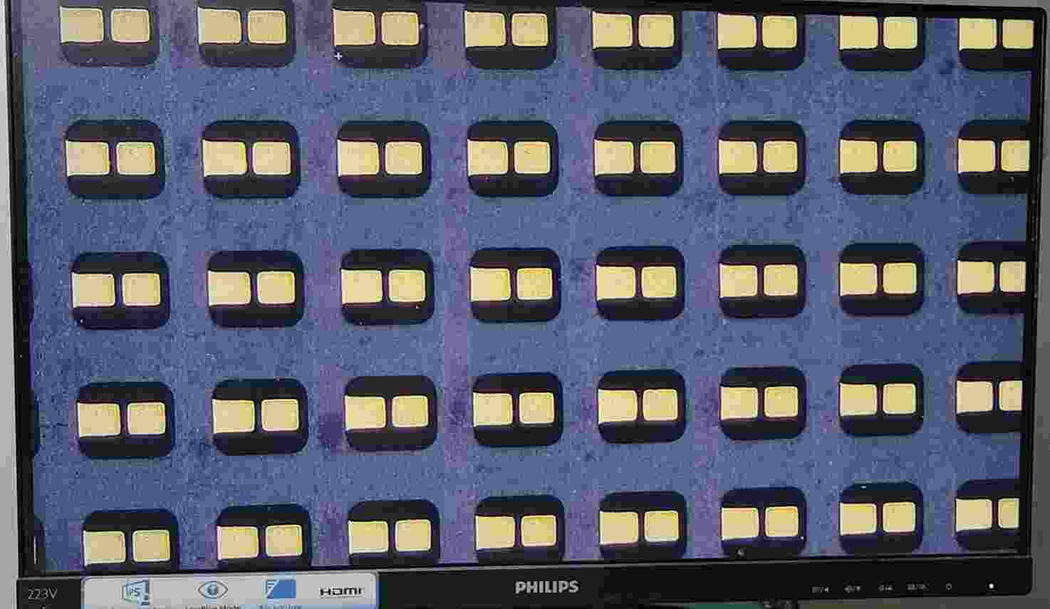
Ultra-small Trace/Spacing LED PCB (Black core and Black soldermask)
What is the importance of Ultra-small gap led PCB?
In the continuous development of electronic engineering, the evolution of printed circuit boards (PCBs) has brought breakthroughs to various technologies. One of the eye-catching developments is ultra-fine pitch LED PCB, a technology that is redefining the fields of lighting solutions and electronic displays. In this comprehensive guide, we’ll delve into the intricacies of ultra-fine pitch LED PCBs, covering their structure, functionality, manufacturing techniques, and how they differ from traditional PCBs.
In today’s trend of pursuing thin, light and short electronic devices, ultra-fine pitch LED PCB has become a powerful tool to achieve extremely compact design. Their superior circuit layout and advanced packaging technology enable these PCBs to achieve excellent performance in space-constrained environments, providing an ideal solution for ultra-thin electronic devices.
Especially in the manufacturing of high-resolution displays, ultra-fine pitch LED PCB plays a vital role. Its sophisticated and compact design allows LED elements to be arranged more densely, resulting in higher pixel density. This high-density arrangement not only improves the resolution of the display, but also brings more detailed and vivid image expression.
Moreover, the considerable customizability of ultra-fine pitch LED PCB stands out as a crucial factor. Manufacturers have the flexibility to adjust the size, shape, and layout of PCBs according to specific requirements, catering to the design intricacies of diverse electronic devices. This adaptability unlocks a myriad of possibilities for product design, addressing the varied needs of different markets and users.
In essence, the significance of ultra-fine pitch LED PCB extends beyond its exceptional performance; it also brings about a revolutionary impact on electronic equipment design. Positioned as a cutting-edge technology in electronic engineering, this PCB charts a new course for future innovation, ushering electronic products into a more compact, efficient, and advanced era.
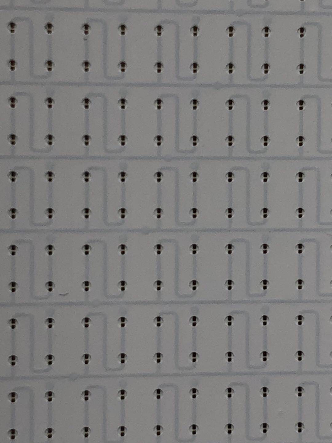
Ultra-small Trace/Spacing LED PCB( White core and White soldermask)
What are the types and classifications of Ultra-small gap led PCB?
Within the realm of electronic engineering, packaging substrates stand out as crucial components responsible for the interconnection and support of electronic elements. Diverse types of packaging substrates are meticulously crafted to meet distinct needs and applications, underscoring the importance of comprehending their classifications and characteristics for the optimization of electronic designs. Notably, the ultra-fine pitch LED PCB has garnered attention in the electronics industry due to its compact design and exceptional performance, making it a noteworthy innovation in this field.
Packaging substrates are classified primarily based on their use and design features. Here are some common packaging substrate types:
BGA (ball grid array) packaging substrate
The BGA package substrate is known for its spherical pad arrangement, which enables higher connection density by increasing the number of connection points and reducing the pad spacing. This provides more design flexibility and performance advantages for high-performance applications, such as ultra-fine pitch LED PCBs.
CSP (Chip Scale Package) Substrate
CSP substrates typically come in smaller, thinner packages that package the chip directly on the substrate, reducing the space required in traditional packaging. This is very important for applications that require extremely miniaturized designs, such as LED PCBs that require ultra-fine pitch.
HDI (High Density Input) Baseboard
HDI substrates use advanced manufacturing technology to achieve higher connection density and smaller size by adding internal layers and adopting micronization processes. This is crucial for realizing high-performance electronic devices in restricted spaces, especially ultra-fine pitch LED PCBs.
Rigid-Flex board
Rigid-Flex substrate is a design that combines rigid and flexible materials to provide greater design freedom. This is very beneficial for applications that require electronic components to be accommodated in complex shapes or restricted spaces, and this design is becoming increasingly popular in ultra-fine pitch LED PCBs.
Understanding the classification and characteristics of these packaging substrates is critical to electronic design. For example, when designing ultra-fine pitch LED PCBs, choosing the appropriate packaging substrate type can optimize the design to the greatest extent and ensure a balance between performance, size and reliability. Through in-depth research and understanding of the characteristics of these packaging substrates, engineers can better cope with the challenges of different application scenarios and promote the development of electronic technology.
Building bridges: What is the difference between Ultra-small gap led PCB
and traditional PCB?
In an era of rapid advances in chip packaging technology, ultra-fine pitch LED PCB, as an innovative evolution of printed circuit boards (PCBs), presents eye-catching differences compared with traditional PCBs. By delving into the classification of chip packaging technologies, similar substrate (SLP), high-density jack (HDI) substrate, and motherboard, we can get a clearer picture of the difference between the two.
First of all, ultra-fine pitch LED PCB has taken a solid step in chip packaging technology. Its unique design makes it possible to accommodate more LED components in a limited space. Compared with traditional PCB, ultra-fine pitch LED PCB uses advanced chip packaging technology to integrate LED chips more compactly, thereby achieving higher pixel density and better display effects.
The introduction of similar substrate (SLP) adds a lot to ultra-fine pitch LED PCB. Compared with traditional PCB, SLP uses more advanced materials and manufacturing processes to achieve a thinner and lighter design. This enables ultra-fine pitch LED PCBs to be widely used in thin and light electronic devices, such as ultra-thin TVs, mobile phones and electronic signage.
The use of high-density jack (HDI) substrate further enhances the performance of ultra-fine pitch LED PCB. HDI technology increases the connection density of circuit boards by adding more layers and smaller apertures in a limited space. This increase in density means more signal paths and more complex circuit designs, providing greater flexibility and performance advantages for ultra-fine pitch LED PCBs.
At the same time, ultra-fine pitch LED PCB also shows unique features in motherboard design. Traditional motherboards often face space constraints and heat dissipation challenges, while ultra-fine pitch LED PCBs effectively solve these problems through sophisticated design and advanced heat dissipation technology. This enables ultra-fine pitch LED PCBs to have better performance in large electronic displays and LED video walls, bringing users a more shocking visual experience.
Generally speaking, the innovation of ultra-fine pitch LED PCB in chip packaging technology, SLP, HDI substrate and motherboard makes it more advantageous than traditional PCB. This advantage is not only reflected in the compact design and high-performance display effect, but also in the wide range of applications that can be adapted to various types of electronic equipment. The new characteristics of ultra-fine pitch LED PCB will continue to lead the development trend of electronic engineering and provide broader space for future innovation.
Explore Ultra-small gap led PCB manufacturing technology?
As an important innovation in the field of electronic engineering, ultra-fine pitch LED PCB’s core value lies in its precise and complex structure and the advanced production technology used. In this section, we will delve into the manufacturing process of ultra-fine pitch LED PCBs, involving improved HDI manufacturing methods and innovative semi-additive manufacturing processes, revealing how these technologies make these PCBs stand out in the market.
Improved HDI manufacturing methods
The manufacturing of ultra-fine pitch LED PCB begins with the continuous improvement of HDI manufacturing methods. High-density jack (HDI) technology is designed to increase the density of components that can be placed on a PCB, thereby enabling smaller size and higher-performance electronic devices. By adopting improved HDI manufacturing methods, ultra-fine pitch LED PCB can achieve a more compact design, allowing LED components to be arranged and connected more effectively in a limited space.
This technological innovation not only improves the integration of components, but also significantly reduces resistance and inductance, providing a solid foundation for improving the performance of LED equipment.
Innovative semi-additive manufacturing process
Another manufacturing highlight of ultra-fine pitch LED PCB is the innovative application of semi-additive manufacturing process. This process introduces an advanced manufacturing method that accurately builds the circuit structure by adding materials layer by layer on the PCB. Compared with the traditional full additive process, the semi-additive process is more refined and flexible.
Semi-additive manufacturing processes allow thin films to be added layer by layer in specific areas, allowing for greater control over the layout and properties of circuits. This precision is the basis for achieving key features of ultra-fine pitch LED PCBs, as the dense layout and high integration of LED components requires higher precision and flexibility in the PCB manufacturing process.
The pinnacle of ultra-fine pitch LED PCB manufacturing technology
Combining the improved HDI manufacturing method with the innovative semi-additive manufacturing process, ultra-fine pitch LED PCB has reached a peak state in manufacturing technology. The synergy of these two technologies allows these PCBs to achieve more functionality and higher performance in a relatively small space. As a result, ultra-fine pitch LED PCBs are ideal for modern electronic devices and displays, providing users with more advanced and compact solutions.
By delving into these advanced manufacturing technologies, we can better understand how ultra-fine pitch LED PCBs stand out in design, bringing new possibilities for innovation in the electronics field. The subtlety of this manufacturing process lies in its continuous evolution. With the continuous development of technology, the future of ultra-fine pitch LED PCB will be full of more exciting innovations.
Explore Ultra-small gap led PCB FAQs
As an innovative technology in the electronics field, ultra-fine pitch LED PCB has aroused widespread interest among amateurs and professional practitioners.
What is ultra-fine pitch LED PCB?
Ultra-fine pitch LED PCB is a printed circuit board with an extremely compact design designed to enable highly integrated LED technology. It is unique in its ability to provide excellent display effects, making it ideal for high-resolution electronic devices.
What is the difference between ultra-fine pitch LED PCB and traditional PCB?
Compared with traditional PCBs, ultra-fine pitch LED PCBs are more precisely designed to achieve higher pixel density and narrower pitches. This gives them a clear advantage in the field of large screens and high-definition displays.
Why ultra-fine pitch LED PCB is suitable for high-resolution display?
The reason why ultra-fine pitch LED PCB is suitable for high-resolution display devices mainly benefits from its compact design and advanced manufacturing technology. This allows LED pixels to be arranged more densely, providing more detailed and clear images, thus meeting the requirements for high-resolution displays.
What are the manufacturing technologies for ultra-fine pitch LED PCB?
The manufacturing of ultra-fine pitch LED PCBs involves a variety of technologies, including improved high-density inlet (HDI) manufacturing methods and innovative semi-additive manufacturing processes. The combination of these technologies enables ultra-fine pitch LED PCBs to achieve smaller physical spacing while maintaining high quality.
What application areas are ultra-fine pitch LED PCB suitable for?
This advanced PCB technology is widely used in large TV screens, display walls, monitors and other situations where high resolution and detailed images are required. Its excellent display makes it an ideal choice for business, entertainment and surveillance.
How to choose ultra-fine pitch LED PCB suitable for your project?
Choosing an ultra-fine pitch LED PCB suitable for a project requires considering many factors, including the project’s display requirements, environmental conditions, and budget. Professionals recommend fully understanding the product specifications and performance characteristics of different manufacturers before choosing to ensure that you choose the PCB that best suits your project.
What is the future development trend of ultra-fine pitch LED PCB?
A semiconductor packaging substrate, commonly referred to as a packaging substrate, holds a pivotal role in the realm of electronics by serving as a vital component responsible for transporting, interconnecting, and safeguarding semiconductor chips. It furnishes the essential support structure that links minuscule chips to the circuit board, thereby establishing a robust foundation for the proper operation of electronic devices. Packaging substrates are versatile and can be crafted from various materials, including rigid substrates, flexible substrates, or high-performance polymers, each tailored to meet distinct application requirements.