 Professional Flip-Chip Packaging Substrate Supplier


 Substrate")

Why CHOOSE SHENZHEN QYC CO.,LTD?
We mainly produce high quality high layer packaging substrates from 2 layers to 20 layers. The types of substrates are:3D IC Package Substrate, 2.5D IC Package Substrate, 2D IC Package Substrate, FCLGA Package Substrate, FCCSP Package Substrate, FCBOC Package Substrate, FCPBGA Package Substrate, FCPGA Package Substrate, WBBGA Package Substrate, WBCSP Package Substrate, WBBOC Package Substrate, RF Module Package Substrate, Digital Module Package Substrate, WLP Package Substrate,POP Package Substrate,SIP Package Substrate,SOP Package Substrate,Ball Grid Array Package Substrate,LCC Package Substrate,DIP Package Substrate,QFP Package Substrate, , or Packaging service. and we also produce Microtrace HDI PCBs. Such as: Microtrace LED PCBs, Microtrace Rogers PCBs.
When you are designing Packaging Substrate, if you have doubts about the substrate production process, or are not sure whether the factory can perfectly realize your design requirements, we are ready to provide you with consultation and support. Please feel free to contact us via email and our team of professional engineers will answer you promptly. To ensure that your design is optimally executed and realized, we are always committed to working closely with designers to identify and solve process or technical problems encountered by designers. We have a team of more than 200 professional engineers, and about 100 to 200 new customers from all over the world establish cooperative relationships with us every month. Some of our customers chose us through online searches, while others came through enthusiastic recommendations from our long-term customers. The reason why we can win the trust of our customers is not only because we always maintain stable and high quality, but also because we use high-precision production machinery and equipment. We always use designated brands of materials in accordance with the customer's specific instructions, ensuring that each product perfectly fits the customer's expectations and requirements. Our persistence and focus are the key to consistent quality.
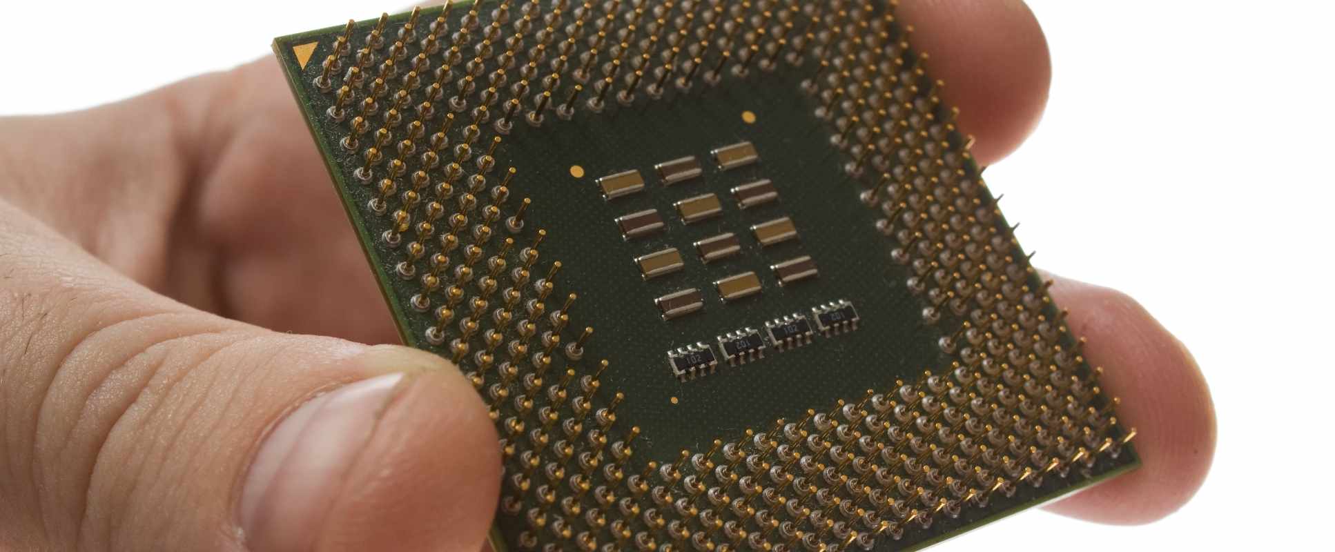
FC-BGA substrates
FC-BGA substrates
FC-BGA (Flip Chip Ball Grid Array) is a technology used for high-density semiconductor packaging. By flipping the chip onto the packaging substrate, it effectively provides more connection points, allowing high-speed chips to achieve more functions. This kind of packaging also allows communication products to use high-frequency materials to improve the performance and stability of signal transmission. In summary, FC-BGA brings high-density, high-performance packaging solutions to the semiconductor industry, helping to meet the growing demand for functionality and performance in modern electronic devices.
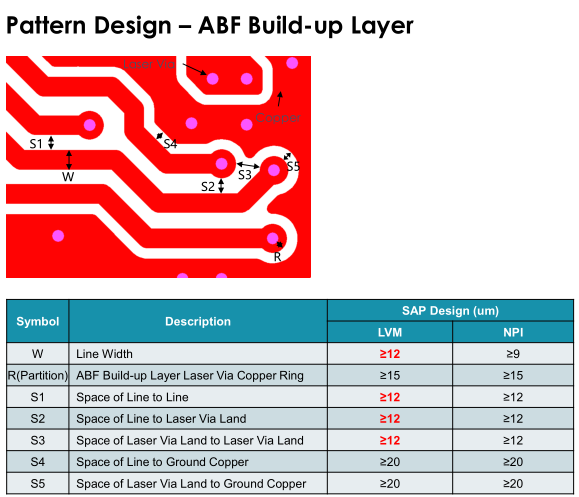
Currently, we have successfully produced multi-layer high-density substrates with 10 to 18 layers. These substrates use Msap (Micro-Structured Surface Finish) or Sap (Surface Activation Process) technology to meet the requirements of small spacing and small line width, providing strong support for current semiconductor micro-manufacturing. These advanced technologies and high-density designs help advance the semiconductor industry, providing electronic devices with higher performance and more functionality.
Our main products are targeted at multiple industries, including servers, artificial intelligence (AI), networking, communications, military industry, and aviation. Product types:IC Substrates. FC-BGA substrates. SHDBU substrates. FC-CSP Substrates. CPCORE Substrates. Module Substates. MSD substrates, FR substrates, SEN substrates , MIC substrates and others.We provide our customers with comprehensive support from substrate design to production, even packaging. In terms of substrate manufacturing, we insist on using designated brands of materials to ensure product quality and reliability. This focused approach to quality enables us to meet the needs of various industries for high-performance, high-reliability electronic solutions. Our team is committed to providing customers with superior technology and support to meet evolving market needs.
Read more +
WHO ARE WE?
 We are the industry's leading Flip Chip Package Substrate production company. So far, we have more than 10,000 unique team members, and we continue to grow our professional team with steady development. This not only demonstrates our industry strength, but also heralds our company’s broader development potential in the future.
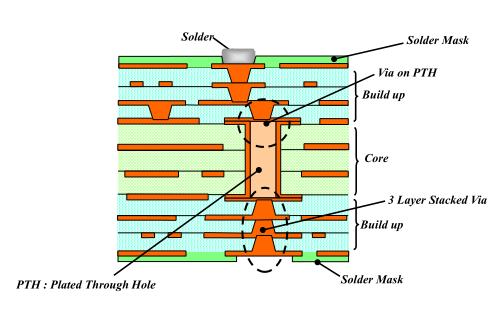
Our company relies heavily on Japan's advanced high-precision production equipment to manufacture FC BGA substrate. This ensures the excellent quality of the package substrate we produce. Through these top-notch equipment, we promise to provide the most perfect product quality, and the quality is always stable, bringing unparalleled reliability to our customers. Currently, our company has produced many 4- to 18-layer Flip Chip Package Substrates. In particular, for complex Flip Chip Package Substrates such as 14-layer ABF materials, we can ensure their quality with efficient productivity. We are proud that our production cycle is only 1 to 2 months, ensuring extremely fast delivery. Such short production time and fast delivery do not compromise our pursuit of product quality - every Substrate reaches perfect manufacturing standards, demonstrating our excellent craftsmanship and technical strength.
When it comes to material selection for Package Substrate, we have multiple sources, including top suppliers in Japan, South Korea, Taiwan and China. Based on the specific needs of our customers, we carefully select and use the most appropriate materials to manufacture Substrate, ensuring that each product accurately meets customer expectations and standards.