 Professional Flip-Chip Packaging Substrate Supplier

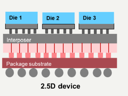
What is 2.5D IC packaging substrate?
Semiconductor 2.5D IC Package Substrate manufacturer and 2.5D IC Package service .High speed and high frequency material packaging substrate manufacturing. Advanced packaging technology.
2.5D IC packaging substrate is an innovative packaging technology designed to integrate multiple chips or chip levels onto a single substrate to achieve superior performance and functional improvements. In PCB engineering, they mark a new milestone in packaging technology, bringing revolutionary changes to the design and manufacturing of electronic devices.
In traditional packaging methods, each chip is usually packaged in a separate package, while 2.5D IC packaging substrates bring new possibilities to system design by integrating multiple chips on the same substrate. Its main functions are reflected in the following aspects:
Performance improvement: 2.5D IC packaging substrate greatly improves the connection speed and bandwidth between chips, while reducing the delay and loss of signal transmission. This more efficient connection provides the system with faster data transfer rates and lower power consumption, resulting in superior performance.
Rich functions: By integrating multiple chips on the same substrate, 2.5D IC packaging substrates provide greater integration and richer functions for the system. Chips with different functions can work together on the same packaging substrate, thereby reducing system complexity and improving overall efficiency and reliability.
Space optimization: Compared with traditional packaging methods, 2.5D IC packaging substrates can achieve a more compact design, effectively saving system space. This space optimization not only makes the equipment more compact and lighter, but also provides designers with greater flexibility and creativity, promoting product innovation and development.
In general, 2.5D IC packaging substrate represents a new generation of packaging technology, which greatly improves the performance, functionality and design flexibility of the system, and opens up new prospects for the development of electronic equipment.
What are the types of 5D IC packaging substrates?
In modern PCB engineering, 2.5D IC packaging substrates cover a variety of types, each with unique characteristics and applications. Let’s take a deeper look at these types and explore the differences between them.
The silicon interlayer substrate uses silicon as the substrate material, which is characterized by high bandwidth, low delay and excellent electrical properties. This type of substrate is suitable for applications requiring high-speed signal transmission, such as high-performance computing and communication systems. Silicon interlayer substrates have a higher cost compared to other types but excel in performance.
The glass interlayer substrate uses glass as the substrate material and has excellent thermal conductivity and reliability. This type of substrate is particularly suitable for high-power applications such as automotive electronics and industrial control systems. Glass interlayer substrates are more cost-competitive than silicon interlayers and maintain stable performance in high-temperature environments.
Organic interlayer substrates use organic materials and are a cost-effective packaging solution with good signal integrity and thermal performance. This type of substrate is commonly used in consumer electronics and general computing applications where both cost and performance are required.
These different types of 2.5D IC packaging substrates differ in materials, performance and cost, so selection needs to be weighed based on the requirements of the specific application. No matter which type of substrate is chosen, multi-chip integration can be achieved through 2.5D technology to improve system performance and meet the growing demand for electronic devices.
What are the advantages of 2.5D IC packaging substrate?
As an advanced packaging solution, 2.5D IC packaging substrate has many significant advantages over traditional packaging methods, which make it widely adopted. Below we will explore these advantages to better understand why 2.5D IC packaging substrates are so popular.
2.5D IC packaging substrate can realize multi-chip integration. By integrating multiple chips on the same substrate, high-speed interconnection can be achieved, thus greatly improving the performance of electronic equipment. Compared with traditional packaging methods, this increase in integration makes signal transmission more efficient, reduces signal loss and delay, and significantly improves the overall performance of the system.
The 2.5D IC packaging substrate uses advanced packaging technology to achieve a more compact design, thereby miniaturizing and lightweighting the device. Since multiple chips can be integrated on the same substrate, no additional space is needed to accommodate multiple independent packages, so more compact products can be designed, which is suitable for applications with strict size and weight requirements.
The 2.5D IC packaging substrate performs well in thermal management and can conduct and dissipate heat more effectively, ensuring the reliability and stability of the device under high load conditions. By using materials with high thermal conductivity and well-designed heat dissipation structures, 2.5D IC packaging substrates can effectively reduce chip operating temperatures, extend the service life of equipment, and reduce failure rates.
The 2.5D IC packaging substrate realizes the tight integration of multiple chips, greatly improving the integration density of the system. By integrating multiple chips and components on the same substrate, more complex and feature-rich electronic systems can be realized, reducing the complexity of internal connections in the system and improving the reliability and stability of the overall system.
Although 2.5D IC packaging substrates may be higher in terms of initial investment, their superior performance and miniaturized design will bring long-term cost benefits in the long run. By improving equipment performance, reducing energy consumption, reducing failure rates and simplifying system design, 2.5D IC packaging substrates can bring significant economic benefits to enterprises and improve overall competitiveness.
To sum up, 2.5D IC packaging substrate has become a favored packaging solution in the field of electronic device design today due to its excellent performance, miniaturized design, optimized thermal management, high integration density and cost-effectiveness. With the continuous advancement of technology and the expansion of its application scope, it is believed that it will play an increasingly important role in the future and promote the development of the electronics industry.
Why choose 2.5D IC packaging substrate?
In modern PCB engineering, selecting the appropriate packaging substrate is crucial to achieving high performance and functional electronic devices. Compared with traditional packaging boards, 2.5D IC packaging substrates present unique advantages, making them a favored choice by many engineers and designers.
First, 2.5D IC packaging substrates provide excellent performance advantages. By integrating multiple chips onto a single substrate, 2.5D technology enables high-speed interconnection, thereby reducing signal loss, increasing bandwidth, and reducing power consumption. This highly integrated design helps improve system performance, achieve faster data transfer rates and lower energy consumption, allowing the device to perform well in different application scenarios.
Secondly, the 2.5D IC packaging substrate has excellent miniaturization characteristics. Compared with traditional packaging methods, 2.5D technology can achieve higher device integration density, thereby achieving smaller device size and lighter product design. This miniaturization advantage allows electronic devices to be more compact and suitable for applications with strict size and weight requirements, such as portable consumer electronics and medical equipment.
In addition, the 2.5D IC packaging substrate has excellent thermal management capabilities. Due to the tight integration between chips, 2.5D technology helps improve heat conduction efficiency, effectively dispersing heat to the substrate surface and dissipating it through the heat dissipation structure, thereby maintaining stable performance of the device under high load conditions. This superior thermal management capability makes 2.5D IC packaging substrates ideal for high-power applications such as data centers, automotive electronics, and industrial control systems.
In addition, 2.5D IC packaging substrates also provide greater design flexibility. Compared with traditional packaging methods, 2.5D technology can realize the integration of heterogeneous chips, that is, chips with different manufacturing processes or functions can be integrated on the same substrate. This flexibility provides engineers with more design options, allowing them to better optimize system performance and implement more diverse product features.
In summary, compared with other packaging boards, choosing 2.5D IC packaging substrates has many advantages. Its excellent performance, miniaturization, excellent thermal management capabilities and design flexibility make it one of the indispensable key technologies in the design of today’s electronic equipment. With the continuous advancement of technology and the continuous demand of the market, 2.5D IC packaging substrates will continue to play an important role and promote the continuous innovation and development of the electronics industry.
2.5D IC Package Substrate
What is the manufacturing process of 2.5D IC packaging substrate?
Manufacturing 2.5D IC packaging substrates is a complex and precise process that involves multiple critical steps to ensure high performance and reliability of the final product. The following is the general process of manufacturing 2.5D IC packaging substrate and its key steps:
Detailed design and planning work is required before the manufacturing process can begin. This includes determining the packaging solution, selecting the appropriate packaging technology, designing the circuit layout, etc. The key at this stage is to ensure that the design meets performance and functional requirements and takes into account feasibility during manufacturing.
The materials required to manufacture 2.5D IC packaging substrates include substrate materials (such as silicon, glass or organic matter), chips, metallization layers and packaging compounds. These materials must be precisely selected and processed to ensure they meet process requirements and achieve good electrical and thermal properties.
The next step in the manufacturing process is to prepare the substrate. This may involve surface preparation, cleaning and chemical treatments of the substrate to provide good adhesion and conductivity. For silicon substrates, processes such as wafer cutting and polishing may also be required.
Once the substrate is ready, the chip can be placed on the substrate and connected. This is typically connected via flip-chip mount or via through-silicon vias (TSVs). Chip placement and connections must be very precise to ensure circuit stability and reliability.
After connecting the chip, the package needs to be encapsulated and encapsulated. This may involve applying encapsulation material between the chip and the substrate to provide protection and mechanical support and ensure a stable connection. The choice of packaging material must take into account its impact on electrical and thermal properties.
The final step in the manufacturing process is testing and verification of the packaging substrate. This includes comprehensive testing of electrical, thermal and mechanical properties to ensure the package substrate meets specifications and performance requirements.
Through these key steps, manufacturing 2.5D IC packaging substrates can achieve a high degree of accuracy and reliability, providing superior performance and functionality for modern electronic devices.
What are the applications of 5D IC packaging substrates?
As an advanced packaging technology, 2.5D IC packaging substrate has been widely used in many fields. Its influence is not limited to a single industry, but spans multiple fields and promotes the development of different industries. The following will discuss the application of 2.5D IC packaging substrates in different fields and its promotion of industry development.
In the fields of cloud computing and data centers, the application of 2.5D IC packaging substrates provides a more efficient solution for processing large-scale data. By integrating multiple chips onto a single substrate, processing speeds and data throughput can be increased, thereby accelerating data center computing speed and performance. This high-performance and high-density packaging technology provides a reliable foundation for large-scale data processing and provides important support for the development of cloud computing and data centers.
In the fields of communications and networking, the application of 2.5D IC packaging substrates brings faster and more reliable data transmission. By adopting high-density integrated packaging solutions, higher bandwidth and lower latency can be achieved, improving the performance of network equipment and communication systems. The application of this technology provides a more stable and efficient foundation for mobile communications, wireless networks and Internet services, and promotes the advancement and popularization of communications technology.
In the field of automotive electronics, the application of 2.5D IC packaging substrates provides key support for the development of smart cars and autonomous driving technology. By integrating multiple functional modules into a compact package, a high degree of integration and optimization of automotive electronic systems can be achieved, improving the intelligence and safety performance of the vehicle. This advanced packaging technology provides strong technical support for the innovation and development of automotive electronics and promotes the transformation and upgrading of the automotive industry.
In the field of industrial control and automation, the application of 2.5D IC packaging substrates provides important support for factory automation and smart manufacturing. By integrating multiple sensors, processors and communication modules into a compact package, industrial equipment can be intelligent and interconnected, improving production efficiency and product quality. This advanced packaging technology provides new possibilities for the development of industrial control and automation, and promotes the upgrading and transformation of the manufacturing industry.
In summary, 2.5D IC packaging substrates have been widely used in many fields such as cloud computing, communications, automotive electronics, and industrial control, and have significantly promoted the development of different industries. With the continuous advancement of technology and the continuous expansion of application scope, it is believed that 2.5D IC packaging substrates will continue to play an important role in promoting innovation and development in various industries around the world.
Where can I find 2.5D IC packaging substrates?
When looking for reliable 2.5D IC packaging substrates, choosing the right supplier is crucial. As a well-known company, we are committed to providing high-quality packaging substrates that meet the various needs and requirements of our customers. Here are a few reasons why choose us as your supplier of 2.5D IC packaging substrates:
Quality Assurance: Our company has rich experience and expertise and is committed to providing high-quality 2.5D IC packaging substrates. We strictly follow international standards and industry best practices to ensure that each packaging substrate undergoes strict quality control and testing.
Innovation capabilities: As a technology-leading company, we continuously invest funds and resources in research and development and are committed to developing novel packaging solutions. Our engineering team has rich technical background and innovative awareness, and can provide customers with customized 2.5D IC packaging substrate design.
Customer service: We value communication and cooperation with customers and always focus on customer needs. Our sales team and technical support team will wholeheartedly provide you with professional services to solve any problems and difficulties you encounter during the procurement and application of packaging substrates.
On-time delivery: We have advanced production equipment and efficient production processes to ensure on-time delivery of 2.5D IC packaging substrates. No matter how urgent your project is, we will do our best to meet your delivery requirements.
Comprehensive support: In addition to providing high-quality 2.5D IC packaging substrates, we also provide comprehensive technical support and after-sales service. Whether you need help with design, manufacturing or applications, we’re here to provide support and guidance.
To sum up, choosing us as your 2.5D IC packaging substrate supplier will bring you reliable product quality, innovative solutions and excellent customer service experience. We look forward to establishing a long-term cooperative relationship with you and jointly promote the development and progress of the electronics industry.
What is the quotation for 2.5D IC packaging substrate?
If you want to get a quote for a 2.5D IC packaging substrate, you need to consider a series of factors, which directly affect the price of the substrate. Here are some key factors and their impact on price:
Different types of 2.5D IC packaging substrates have different performance and functional characteristics, so the prices will also be different. For example, substrate types such as silicon interposers, glass interposers and organic interposers have differences in material cost, manufacturing process and performance, so prices will fluctuate.
The specifications and dimensions of the substrate play a crucial role in cost. Larger substrate sizes typically require more materials and processing steps, so the price increases accordingly. Additionally, special custom substrate specifications may result in additional customization costs.
The number of substrates ordered also has an impact on the price. Generally speaking, the unit cost of mass-produced substrates is low, while the cost of small-batch production is relatively high. Therefore, ordering substrates in large quantities may lead to more competitive pricing advantages.
Certain technical requirements may increase the complexity of the manufacturing process, thereby affecting price. For example, if the substrate requires special lamination techniques or a higher-precision manufacturing process, additional process steps and equipment may be required, which will be reflected in the final quote.
Different suppliers may provide 2.5D IC packaging substrates of different qualities and prices. Choosing a reliable supplier ensures product quality and delivery time and may affect the final price. It is often recommended to compare with multiple suppliers and consider their reputation, production capabilities, and customer service.
To sum up, obtaining an accurate quotation for 2.5D IC packaging substrate requires comprehensive consideration of the above factors. By understanding these key factors, and communicating and comparing with multiple suppliers, you can better determine the product that suits your needs and obtain the most competitive price.
Frequently Asked Questions (FAQs)
How do 2.5D IC Package Substrates differ from traditional packaging methods?
2.5D IC Package Substrates integrate multiple chips onto a single substrate using interposer technology, enabling enhanced performance and miniaturization compared to traditional methods, which often involve separate packaging for individual chips.
What are the key advantages of 2.5D IC Package Substrates?
2.5D IC Package Substrates offer several advantages, including improved performance, miniaturization, enhanced thermal management, and higher integration density, making them ideal for advanced electronic applications.
What industries benefit from the use of 2.5D IC Package Substrates?
Various industries, including high-performance computing, telecommunications, automotive electronics, and aerospace, benefit from the superior performance and integration capabilities offered by 2.5D IC Package Substrates.
What considerations should be taken into account when designing with 2.5D IC Package Substrates?
Designers should consider factors such as substrate material, interconnect technologies, thermal management, and signal integrity to optimize the performance and reliability of systems utilizing 2.5D IC Package Substrates.
Are there any reliability concerns associated with 2.5D packaging?
While 2.5D IC Package Substrates offer numerous benefits, potential reliability concerns may arise from interconnect reliability, thermal issues, and manufacturing complexities, which must be addressed through rigorous testing and design optimization.
How do 2.5D IC Package Substrates compare to 3D packaging technologies?
2.5D IC Package Substrates typically involve the integration of chips on a single plane with an interposer, whereas 3D packaging technologies stack chips vertically, offering different advantages and design considerations depending on the application requirements.