 Professional Flip-Chip Packaging Substrate Supplier

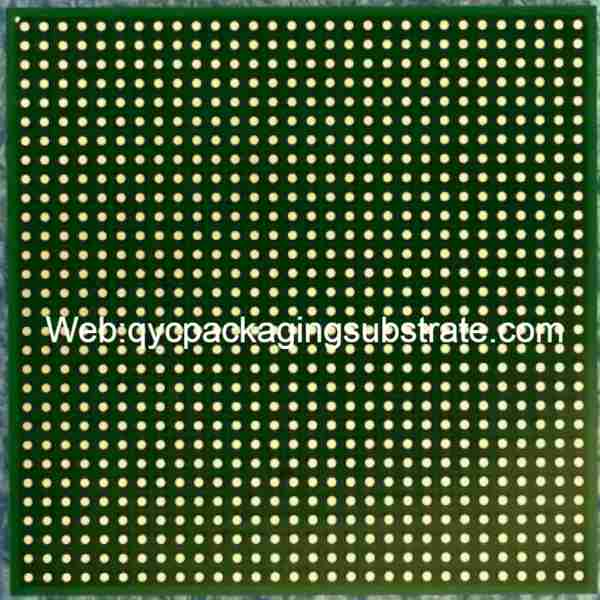
Professional Semiconductor packaging substrate Company, we mainly produce ultra-small bump pitch package substrate and PCBs.
In the modern landscape of electronic design and manufacturing, semiconductor packaging substrates play a crucial role as fundamental components, serving as the foundation for sophisticated Printed Circuit Boards (PCBs). Their primary purpose is to enable seamless integration of electronic components by facilitating electrical connections between semiconductor chips and the overall PCB structure.
These substrates essentially act as bridges within electronic devices, establishing connections between semiconductor chips and other electronic elements to ensure their collaborative functionality. Beyond providing physical support, semiconductor packaging substrates also furnish essential channels for electrical connections among electronic components.
Semiconductor packaging substrates boast a notable feature – the presence of multiple electrical connection points strategically arranged on their surface, establishing links to pins on the semiconductor chip through minute wires. This unique design facilitates the smooth flow of electric current between the semiconductor chip and other components, fostering cohesive operation among diverse parts.
Essential in enabling the seamless integration of electronic components, these substrates provide reliable electrical connections that allow different components to function harmoniously on a single circuit board. This integration is pivotal for the development of more intricate and high-performance electronic devices.
Through meticulous layout and design, these substrates can optimize the performance of electronic systems, ensuring the dependable and efficient collaboration of various components.
In summary, semiconductor packaging substrates play an indispensable role in the design and manufacturing of advanced PCBs. Beyond serving as a medium for connecting electronic components, they represent a critical link in achieving the high performance, miniaturization, and multifunctionality of electronic equipment. In the realm of electronic engineering, a profound understanding and judicious application of semiconductor packaging substrates are poised to be key drivers of future electronic innovation.
Semiconductor packaging substrate quote
What are the types of semiconductor packaging substrates?
Semiconductor packaging substrates, serving as the central element in sophisticated circuit boards, are integral to electronic design. A comprehensive exploration of diverse substrate types, ranging from the intricacies of high-density interconnect (HDI) to the adaptability of organic substrates, presents electronics engineers with a plethora of choices. This array of options is essential for addressing specific design requirements, paving the way for a transformative era of innovation in the field.
High Density Interconnect (HDI) Substrate
High-density interconnect substrate is a technological pinnacle in semiconductor packaging that improves circuit board performance and reliability by enabling more connection points in a limited space. Its complexity is reflected in the design of interlayer connections, microscopic lines and micropores, making it ideal for high-performance electronic devices.
Organic substrates, often constructed from FR-4 (fiberglass reinforced epoxy resin), are extensively employed in various applications due to their advantageous mechanical and electrical characteristics. These substrates, primarily composed of affordable materials, are widely utilized in a diverse array of industries, including but not limited to consumer electronics and industrial control.
Rigid-flexible substrates provide a versatile solution by combining the advantageous characteristics of rigidity and flexibility. Tackling the issue of inflexibility associated with rigid substrates, these materials feature a rigid section that can accommodate components, coupled with a flexible connector at the other end, allowing for bending in confined spaces. This innovative design is prevalent in applications such as mobile devices and medical equipment.
Passive substrate
Passive substrates are usually stacked in multiple layers and do not contain any electrical components. It provides designers with greater freedom to lay out circuits and components, and is suitable for applications with higher requirements on circuit layout, such as RF and microwave equipment.
Flexible substrates feature flexible substrates that maintain performance despite bending and bending. This type of substrate is commonly used in applications that require flexible electronic solutions, such as wearable devices and curved screens.
Various semiconductor packaging substrates offer a wide range of options in electronic design, each showcasing distinct advantages in different situations. Engineers can select the most appropriate solution from these innovative substrate types to cater to specific project requirements, thereby contributing to the ongoing progress of electronic technology.
What are the advantages of semiconductor packaging substrates?
Semiconductor packaging substrates play a vital role in contemporary circuit board design, serving as a fundamental element in electronic engineering and playing a key role in the performance and dependability of electronic devices. This article delves into the numerous benefits of semiconductor packaging substrates, shedding light on their influence on electrical performance, efficient space utilization, and effective thermal management. These advantages collectively contribute to elevating the overall quality and reliability of electronic equipment.
Through the application of high-density interconnect (HDI) technology and advanced manufacturing processes, these substrates facilitate tighter connections between electronic components, reducing signal transmission paths. This optimization directly translates into improved electrical performance, resulting in enhanced response speed and reduced power consumption. The end result is a superior user experience for individuals interacting with the electronic device.
Furthermore, semiconductor packaging substrates excel in space optimization, a critical advantage as electronic devices continue to shrink in size. Effectively utilizing limited space through features such as multi-layer stacking and compact designs, these substrates contribute to the miniaturization of electronic devices. This responsiveness to the demand for portable and thin devices aligns with the evolving preferences of modern consumers, making semiconductor packaging substrates essential in meeting these expectations.
One distinctive feature of semiconductor packaging substrates is their outstanding thermal management capabilities. In high-performance electronic equipment, heat generation is a common challenge, and effective thermal management is crucial for ensuring stable operation. Semiconductor packaging substrates address this by incorporating materials with excellent thermal conductivity and implementing precise heat dissipation designs. This strategic approach allows for the efficient conduction and dissipation of heat, thereby maintaining the device’s temperature within a controllable range. The result is not only enhanced equipment reliability but also an extended operational lifespan.
In conclusion, semiconductor packaging substrates stand out for their contributions to improved electrical performance, space optimization, and superior thermal management. Serving as a cornerstone in modern electronic engineering, these substrates drive continuous innovation and progress in electronic equipment. The combined impact of these advantages underscores the indispensable role of semiconductor packaging substrates in advancing the field and ensuring the ongoing excellence and reliability of electronic devices.
Why choose semiconductor packaging substrate instead of other circuit boards?
In the contemporary landscape of electronic design and manufacturing, there is a growing focus on the evolving significance of semiconductor packaging substrates. This heightened attention is fueled by the distinct advantages these substrates offer compared to traditional printed circuit boards (PCBs). Delving into the rationale behind choosing semiconductor packaging substrates amidst a myriad of circuit board options becomes imperative to appreciate their transformative role in the industry.
Adaptability to advanced technology
Semiconductor packaging substrates stand out for their excellent adaptability to advanced technologies. These substrates offer higher density, more advanced interconnect technology, and better performance than traditional circuit boards. Under the requirements of the new generation of electronic equipment, semiconductor packaging substrates provide stronger support for products with their advanced technical characteristics.
Advantages of space utilization
With the trend of modern electronic equipment pursuing thinner, lighter and smaller sizes, semiconductor packaging substrates perform particularly well in terms of space utilization. Its compact design allows electronic products to be lighter without sacrificing performance. Compared with traditional circuit boards, semiconductor packaging substrates are more flexible in space-limited scenarios, providing designers with more innovative possibilities.
Excellent performance in thermal management
Semiconductor packaging substrates demonstrate exceptional thermal management performance, a crucial aspect as electronic devices continually enhance their functionality. Addressing the escalating thermal challenges, these substrates employ cutting-edge heat dissipation technologies to maintain stable temperatures even under heavy workloads. Their superiority over traditional PCBs lies in enhanced reliability within high-temperature environments, establishing them as the preferred choice for heat-sensitive applications.
The impact of advanced manufacturing technology plays a crucial role in the creation of semiconductor packaging substrates. By integrating cutting-edge manufacturing processes, including high-precision equipment and precision materials, there is a notable improvement in manufacturing quality and reliability. This stands in contrast to traditional circuit board manufacturing, where the adoption of advanced technology results in increased production efficiency, reduced defect rates, and the provision of more dependable products for manufacturers and designers.
First choice for specific scenarios
Semiconductor packaging substrates have become the preferred choice in certain scenarios, especially in applications with more stringent performance, volume and thermal management requirements. This includes areas such as high-performance computing, communications equipment, medical instrumentation, and more. Its advantages in these scenarios make it ideal for specific needs.
Semiconductor packaging substrates excel in advanced technology, efficient space utilization, effective thermal management, and cutting-edge manufacturing processes. In the dynamic electronics industry, opting for these substrates is not just a necessary step towards the future; it’s a strategic move to distinguish oneself in the highly competitive market landscape.
How to manufacture semiconductor packaging substrates?
In the realm of contemporary electronic engineering, semiconductor packaging substrates assume an essential role, with a comprehensive grasp of their manufacturing processes being paramount for understanding their exceptional performance and diverse applications. Delving deeper, we uncover the intricacies involved in the production of motherboards and substrates, highlighting the pivotal role advanced technologies play in this intricate manufacturing process.
The production of motherboards stands as a critical component within the broader semiconductor packaging substrate manufacturing process, encompassing two fundamental methods: subtractive and additive. In the subtractive manufacturing process, manufacturers systematically diminish the motherboard material through a series of precise steps to craft the desired circuit structure. The intricacy of this phase lies in achieving meticulous material removal, ensuring the final circuit board aligns with design specifications.
The additive manufacturing process adds materials layer by layer on the motherboard to build complex circuit structures. Advanced materials and technologies play a key role at this stage, ensuring that each layer of the circuit board can meet the needs of highly complex designs.
Substrate manufacturing
The foundation of semiconductor packaging substrates is the manufacturing of their substrates. This stage involves techniques for manufacturing high-density interconnects, as well as the clever use of key materials such as FR-4 and polyimide.
High-density interconnection technology serves as the foundation for substrate manufacturing, enabling the precise connection of electronic components. Through meticulous processes, circuit boards can accommodate a greater number of components, resulting in enhanced circuit density and performance.
Essential to substrate manufacturing are materials like FR-4 and polyimide, which contribute significantly to the process. These materials boast excellent insulation properties and high temperature resistance, ensuring that semiconductor packaging substrates can operate reliably in extreme working conditions. The careful selection of these materials is crucial in establishing the reliability and stability of the circuit board.
A profound understanding of motherboard and substrate manufacturing processes is essential for comprehending the intricacies of semiconductor packaging substrates. This knowledge underscores the critical role that advanced technologies play in achieving precision during manufacturing. These sophisticated processes form the basis for the exceptional performance of semiconductor packaging substrates in contemporary electronic devices.
What are the applications of semiconductor packaging substrates?
Semiconductor Packaging Substrates play a pivotal role in the healthcare sector, facilitating the development of advanced medical devices. From diagnostic equipment to wearable health monitors, these substrates contribute to the precision and reliability of electronic components in medical applications.
Industrial Automation:In the realm of industrial automation, Semiconductor Packaging Substrates are instrumental in the design of control systems, sensors, and robotic applications. Their ability to handle complex circuits and interface with various sensors makes them indispensable for enhancing efficiency in industrial processes.
Telecommunications:Telecommunication infrastructure relies heavily on Semiconductor Packaging Substrates for the development of network equipment, routers, and communication devices. The high-performance capabilities of these substrates contribute to the seamless transmission of data in telecommunications networks.
Aerospace and Defense:Semiconductor Packaging Substrates play a critical role in aerospace and defense applications, where reliability and durability are paramount. These substrates are utilized in avionics, radar systems, and communication devices for their ability to withstand harsh environmental conditions.
Communication Devices: Semiconductor packaging substrates are core components in various communication equipment. Base stations, routers, fiber optic communication equipment, and more rely on these substrates to ensure high-speed data transmission and stable communication connections. The advanced manufacturing technology of these substrates provides superior performance for communication equipment.
The widespread application of semiconductor packaging substrates extends beyond these fields to include aerospace, energy, security, and other industries. With their excellent design and manufacturing quality, these substrates inject strong momentum into the development of modern electronic devices. Regardless of the industry, these substrates have become indispensable supporters of innovation and technological advancement. As technology continues to evolve, semiconductor packaging substrates will continue to play a key role in various fields, paving the way for future electronic device innovation.
Where to find semiconductor packaging substrates?
In the quest for superior semiconductor packaging substrates, identifying dependable and high-quality suppliers stands as a pivotal endeavor. This comprehensive guide aims to lead you through a thorough exploration of esteemed manufacturers and distributors in the industry, placing a special emphasis on the meticulous process of acquiring quotes for semiconductor packaging substrates to empower informed decision-making. With pride, we introduce ourselves as a dedicated supplier committed to furnishing top-tier semiconductor packaging substrates.
Identifying Trustworthy Manufacturers and Distributors
As your steadfast supplier for semiconductor packaging substrates, our commitment extends towards building a trusting partnership. We present an insight into our company’s background and its prominent position in the industry to showcase our dedication to providing substrates of unparalleled quality. This includes detailed information about our manufacturing processes, stringent quality control standards, and valuable customer feedback.
Navigating the Quote Acquisition Process for Semiconductor Packaging Substrates
In the intricate landscape of semiconductor packaging substrates, pricing stands as a pivotal factor. We provide a comprehensive discussion on the intricacies of obtaining precise and competitive quotes, enabling you to make judicious decisions. This involves a nuanced consideration of various substrate types, customization requirements, and the nuanced impact of production volumes on pricing.
Choosing Us as Your Preferred Semiconductor Packaging Substrate Supplier
In elevating the conversation, we highlight why entrusting our company with your semiconductor packaging substrate needs is a strategic and advantageous decision. With a strong emphasis on our technological expertise, punctual delivery practices, exceptional customer service, and an unwavering commitment to fostering enduring partnerships, we position ourselves as the ideal collaborator for all your semiconductor substrate requirements.
Informed Decision-Making for Optimal Results
Equipped with a profound understanding of the pivotal role semiconductor packaging substrate suppliers play, you gain the power to make discerning decisions. Opting for our company as your supplier guarantees an assurance of unparalleled quality and reliability for your electronic devices.
Get a quote for semiconductor packaging substrates
This article endeavors to dissect the factors influencing semiconductor packaging substrate quotes, empowering readers to make economically sound decisions.
Impact of Substrate Types
Varied substrate types exhibit significant cost disparities owing to distinct manufacturing processes and material requirements. Notably, HDI substrates entail intricate manufacturing processes and employ high-performance materials, contributing to relatively elevated production costs.
Consideration of Complexity
The intricacy of a substrate directly shapes the technological challenges and costs associated with its manufacturing. Substrates featuring multiple layers, fine circuits, and intricate layouts necessitate advanced manufacturing techniques, potentially resulting in higher production costs. Designers must strike a balance between complexity and performance requirements to ensure optimal cost-effectiveness.
Impact of Production Volume on Pricing
Economies of scale play a pivotal role in semiconductor packaging substrate production. Larger production volumes generally lead to lower average manufacturing costs. Consequently, ordering substantial batches of substrates may yield more competitive prices. Conversely, for small-scale or prototype manufacturing, costs may be relatively higher.
Technological Innovation and Customization Requirements
Technological innovation and customization demands also exert influence on semiconductor packaging substrate pricing. Advanced manufacturing technologies and tailored designs may incur additional costs, but they confer unique competitive advantages.
How much is the quote for semiconductor packaging substrate?
As a key component of modern electronic engineering, the quotation of semiconductor packaging substrates involves many complex factors and requires an in-depth analysis of the cost structure to help make economically informed decisions. Below is an in-depth look at semiconductor packaging substrate quotes.
The Anatomy of Cost Considerations
The cost of semiconductor packaging substrates is not only the direct cost of production, but also includes factors at multiple levels. This covers many factors such as material cost, manufacturing process, technical difficulty, market demand, etc. When evaluating these aspects, manufacturers need to comprehensively consider cost while ensuring quality and performance to ensure that the final quotation can meet market demand.
The impact of substrate type on price
Different types of semiconductor packaging substrates have different performance and application characteristics, and thus their manufacturing and material costs will also vary. High-density interconnect (HDI) substrates have higher requirements in terms of materials and production than traditional substrates, so their quotations are relatively high. Understanding the characteristics of different substrate types helps customers choose the appropriate substrate type according to project needs.
The impact of complexity
The complexity of semiconductor packaging substrates is directly related to the ease of the manufacturing process. Complex designs and highly integrated substrates usually require more sophisticated production processes, resulting in relatively higher costs. The processes, levels and quality controls involved in the manufacturing process all have a direct impact on complexity. Therefore, a deep understanding of the complexities is critical to estimating costs and formulating quotes.
Production volume considerations
Economies of scale play a key role in semiconductor packaging substrate manufacturing. Large-scale production often reduces the manufacturing cost of each substrate, thereby lowering the overall quote. Producers need to carefully evaluate market demand and project size to determine the optimal production volume that can meet market demand while maintaining production efficiency.
Economically sound decisions
It is critical to make a financially sound decision after considering all cost factors. Manufacturers should weigh cost versus performance based on a variety of factors, including project needs, market trends, and budget constraints. Understanding the factors behind a quote and how they impact the final cost can help develop a comprehensive decision-making strategy.
The quotation of semiconductor packaging substrates is not just a number, but contains complex manufacturing processes and multi-level considerations. An in-depth exploration of the factors that influence cost enables customers to better understand the process of forming a quote and make financially informed decisions. In this evolving field of electronic engineering, understanding the cost structure of semiconductor packaging substrates will be one of the keys to success.
Frequently Asked Questions
Are Semiconductor Packaging Substrates adaptable to advanced technologies?
Absolutely. These substrates showcase remarkable adaptability to cutting-edge technologies, making them the preferred choice for electronic designs that demand sophistication and innovation.
How does the manufacturing process differ between motherboard and substrate production?
While motherboard manufacturing involves subtractive and additive processes, substrate manufacturing focuses on creating high-density interconnects. Both processes contribute to the final product’s robustness and efficiency.
What advantages do Semiconductor Packaging Substrates offer?
Semiconductor Packaging Substrates boast advantages such as heightened electrical performance, optimized space utilization, and efficient thermal management. These benefits contribute to the overall efficiency and reliability of electronic devices.
How are Semiconductor Packaging Substrates manufactured?
The manufacturing process involves intricate steps for both motherboards and substrates. Motherboard manufacturing includes subtractive and additive processes, utilizing advanced materials and technologies. Substrate manufacturing employs techniques for creating high-density interconnects and essential materials like FR-4 and polyimide.
What advantages do Semiconductor Packaging Substrates bring to electronic devices?
Semiconductor Packaging Substrates offer heightened electrical performance, enabling faster data transfer and signal integrity. They contribute to space optimization, crucial for modern electronic devices, and exhibit superior thermal management, ensuring optimal functioning under varying conditions.
In what scenarios should one choose Semiconductor Packaging Substrates over traditional PCBs?
Consider Semiconductor Packaging Substrates when aiming for high-density designs, intricate connections, and advanced technologies. These substrates outshine traditional PCBs in scenarios demanding miniaturization and optimal performance.
What is the manufacturing process for Semiconductor Packaging Substrates?
Dive into the complex manufacturing process, encompassing both motherboard and substrate production. Understand the subtractive and additive manufacturing techniques involved, along with the role of advanced materials and technologies in crafting these substrates.