 Professional Flip-Chip Packaging Substrate Supplier

FCBGA Packaging Substrate Manufacturer. Advanced production process and high-precision production equipment can produce 2 to 20 layers of substrate.
in today’s electronic manufacturing field, FCBGA Packaging Substrate plays a vital role. This section will introduce the importance of FCBGA Packaging Substrate in modern electronic manufacturing, and the topics that will be explored in detail in this article, including its characteristics and applications.
FCBGA Packaging Substrate is not only a packaging technology, but also a key component of modern electronic equipment. Its full name, “Ball Grid Array Package Substrate,” implies multiple advantages that are critical in high-performance and high-density electronic manufacturing. Why is it so important?
The Importance of FCBGA Packaging Substrate
First, FCBGA Packaging Substrate supports high-performance and high-density interconnects. It uses a ball grid array connection, which means more connection points can be placed in a smaller space. This provides the possibility for the miniaturization and high integration of modern electronic devices. Whether in smartphones, tablets, or high-performance computing and cloud computing, the high integration of FCBGA Packaging Substrate plays an indispensable role.
Secondly, FCBGA Packaging Substrate has excellent heat dissipation performance. High-performance electronics are often accompanied by greater electrical heat generation. FCBGA Packaging Substrate is designed with this in mind, with its ball grid structure and substrate material helping to conduct and dissipate heat efficiently. This allows it to operate stably under high loads, which is critical for data centers, high-performance computing and communication equipment.
In addition, FCBGA Packaging Substrate excels in signal integrity. Its design reduces the signal transmission path, reducing signal delay and distortion. This is critical for high-speed data transmission and communications equipment as it helps maintain signal integrity and reduce signal loss and noise. Reliable transmission of signals is critical to data accuracy.
Overview of the topic of this article
This article will delve into all aspects of FCBGA Packaging Substrate, including its structure, features, manufacturing process, and applications. We will explore its critical role in high-performance electronic devices and how to meet growing market demands. By understanding the characteristics and applications of FCBGA Packaging Substrate, readers will better understand its indispensability in electronic manufacturing and how to promote innovation in modern electronic equipment.
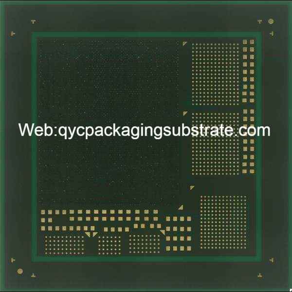
FCBGA Packaging Substrate
What is FCBGA Packaging Substrate?
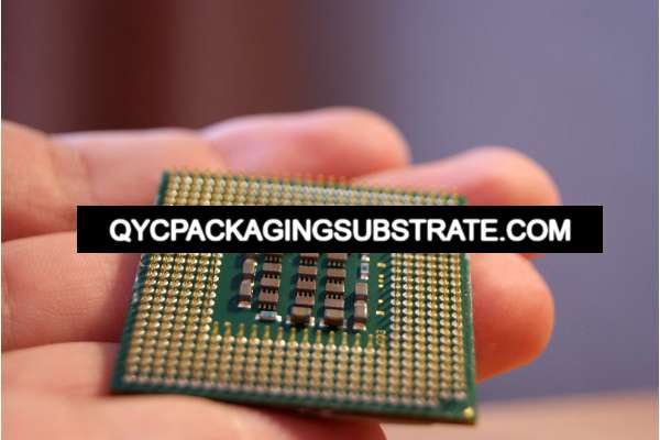
FCBGA Packaging Substrate (ball grid array packaging substrate) represents a key technology in electronic manufacturing. Its abbreviation “FCBGA” corresponds to “Flip Chip Ball Grid Array”, which is “ball grid array packaging substrate”. The name contains the design principles and working methods of FCBGA Packaging Substrate.
Ball Grid Array (Ball Grid Array) is a packaging technology in which chip connection pins are arranged in tiny spherical solder joints on the bottom of the packaging substrate. This design greatly increases connection density, allowing more pins to be connected into a smaller space, providing greater design freedom. This is critical for the high level of integration in modern electronic devices, whether in smartphones or high-performance servers.
Flip Chip refers to the inverted package of the chip, that is, the circuit connection side of the chip faces down and is directly connected to the pins or solder joints on the package substrate. This connection method reduces the signal transmission path, reduces resistance and inductance, helps to increase signal speed and reduce signal delay. This is critical for high-speed data transmission, such as in communications equipment and data centers.
The basic structure and working principle of FCBGA Packaging Substrate
FCBGA Packaging Substrate is usually composed of multi-layer substrates, which can be organic materials, ceramics or high-frequency dielectric materials. Each layer plays a specific role, such as providing electrical connections, heat dissipation, and mechanical support. The chip (IC) is connected upside down to the substrate, and its connection pins are connected to the solder balls on the substrate.
The working principle of FCBGA Packaging Substrate involves circuit connection, heat conduction and signal transmission. Through solder ball connections, electronic signals can be efficiently transmitted to the chip, while electrical heat can be quickly conducted to the substrate and then dispersed to the external environment through its heat dissipation path. This design helps maintain the chip’s temperature within an acceptable range, ensuring high performance and reliability.
In addition, the structure of FCBGA Packaging Substrate also helps maintain signal integrity and reduce loss and interference during signal transmission. This is critical for applications requiring high-frequency signal transmission, such as communications equipment and high-performance computing, as it helps maintain signal integrity and reduce signal loss and noise. Reliable transmission of signals is critical to data accuracy.
These characteristics of FCBGA Packaging Substrate make it one of the preferred packaging technologies for high-performance electronic devices. In the remainder of this article, we will delve into the advantages, manufacturing processes, application areas, and future trends of FCBGA Packaging Substrate to more fully understand its key role in modern electronics manufacturing.
Features of FCBGA Packaging Substrate
FCBGA Packaging Substrate (ball grid array packaging substrate) stands out in modern electronic manufacturing with its unique characteristics and advantages, providing excellent solutions for the packaging of high-performance electronic equipment. This section will delve into the advantages of FCBGA Packaging Substrate over other packaging substrates, with special emphasis on its high-density interconnection, thermal performance and signal integrity characteristics.
High-density interconnection: FCBGA Packaging Substrate is designed to achieve high-density interconnection, which is crucial for the high integration of modern electronic equipment. Through ball grid array connections, FCBGA Packaging Substrate can accommodate more connection points in a smaller packaging space. This high-density interconnect structure provides more circuits and pins than traditional packaging, allowing electronic devices to be designed more compactly. High-density interconnections help improve performance and reduce size to meet the miniaturization and high-level integration needs of modern electronic devices.
Outstanding Heat Dissipation Performance: With advancements in electronic device performance, effective thermal management has become a pivotal concern. The heat generated by high-power chips necessitates efficient dissipation to prevent overheating and potential damage. The FCBGA Packaging Substrate has been purposefully engineered with thermal management considerations. Its ball grid structure and the choice of substrate materials exhibit remarkable thermal conductivity, facilitating the efficient conduction and dissipation of heat. This attribute is of paramount importance for demanding applications like data centers, high-performance computing, and communication equipment.
Signal Integrity: In applications demanding high-speed signal transmission, such as communication equipment and high-performance computing, ensuring signal integrity is of utmost importance. The FCBGA Packaging Substrate minimizes the risk of signal delay and distortion by shortening the signal transmission path. This aids in preserving signal integrity, reducing signal loss and noise, and upholding the reliability of high-speed data transmission. Signal integrity stands as a crucial factor in safeguarding the accuracy and consistency of data transmission.
These characteristics of FCBGA Packaging Substrate make it the preferred packaging technology in high-performance electronic device manufacturing. It not only supports high-density circuit design, but also has excellent thermal management performance and signal transmission quality. In electronics manufacturing, the correct selection of the appropriate packaging substrate type is critical to ensuring product performance and reliability. Next, we will delve into the manufacturing process, application fields and future trends of FCBGA Packaging Substrate to gain a more comprehensive understanding of its key role in modern electronics manufacturing.
FCBGA Packaging Substrate
Quality control of FCBGA Packaging Substrate
In modern electronics manufacturing, quality control is a vital link, especially for key components of high-performance electronic devices such as FCBGA Packaging Substrate. Quality not only affects product performance and reliability, but also is about end-user experience and trust. Therefore, in this section we will emphasize the criticality of ensuring the quality of FCBGA Packaging Substrate, as well as discuss the quality control processes and testing procedures adopted to ensure that the product meets specifications.
The key to ensuring the quality of FCBGA Packaging Substrate
The FCBGA (Flip Chip Ball Grid Array) Packaging Substrate serves as more than just an element within electronic devices; it fulfills several critical roles, including connectivity, data transmission, and thermal regulation. Any compromise in its quality can lead to detrimental consequences, such as unreliable circuit connections, excessive heat accumulation, or signal distortion. These issues subsequently diminish the overall performance and reliability of the entire device. Such setbacks can not only result in product failure but also impact user satisfaction and potentially lead to financial losses. Hence, ensuring the high quality of the FCBGA Packaging Substrate is of paramount importance.
Quality control processes and testing procedures
During the manufacturing process of FCBGA Packaging Substrate, a series of strict quality control measures are adopted. This includes inspection and testing at every stage of manufacturing to ensure the product meets specifications. Here are some common quality control steps and testing procedures:
Lamination inspection: During the lamination process of FCBGA Packaging Substrate, the connections between the layers will be checked to ensure that there are no gaps or damage.
Solder ball connection detection: Solder balls are the key elements connecting the chip and the substrate. They must be soldered correctly and have a good electrical connection. Through the detection of solder ball connections, the quality of the connections can be ensured.
Signal Integrity Testing: These tests involve checking the signal transmission path to ensure signal integrity and accuracy, especially when transmitting at high frequencies.
Thermal performance testing: To guarantee exceptional heat dissipation capabilities of the FCBGA Packaging Substrate when subjected to high workloads, a thermal performance test is conducted to assess its heat conduction and heat dissipation efficiency.
Reliability testing: These assessments replicate product usage in various environmental conditions to verify its enduring stability and reliability over the long term.
Through these quality control processes and testing procedures, manufacturers are able to identify and resolve potential issues, ensuring that each FCBGA Packaging Substrate meets high standards of quality. This helps deliver excellent performance and reliability, providing a solid foundation for the smooth operation of electronic devices.
In the subsequent parts of this article, we will continue to delve into the manufacturing process, application fields and future trends of FCBGA Packaging Substrate to help readers more fully understand the importance of this key component in modern electronics manufacturing.
Future trends of FCBGA Packaging Substrate
FCBGA Packaging Substrate has not only played a key role in the past, but also continues to play a vital role in the face of emerging technologies and market trends. This section will provide an in-depth look at FCBGA Packaging Substrate’s key position in emerging technologies and market trends, and highlight its importance in the evolving electronics manufacturing landscape.
5G technology: With the emergence of 5G wireless communication technology, the demand for high-frequency signal transmission and faster data speeds has increased dramatically. FCBGA Packaging Substrate’s high interconnect density and excellent signal integrity make it ideal for supporting 5G devices. It helps maintain accurate transmission of high-frequency signals, while its heat dissipation performance can meet the heat dissipation needs of high-power 5G equipment.
Artificial intelligence (AI): FCBGA Packaging Substrate’s design and manufacturing process can support high-density, high-performance computing cores, which are critical for AI applications. At the same time, its excellent cooling performance helps ensure that long computing tasks run smoothly.
High-performance computing: The field of high-performance computing requires a large amount of computing resources, and the high-density interconnect structure of FCBGA Packaging Substrate can support more computing cores and memory modules. This makes it the packaging technology of choice for supercomputers, data centers and scientific research equipment.
The continuous evolution of electronic manufacturing: The field of electronic manufacturing continues to evolve, and the continuous emergence of new materials and manufacturing technologies poses new challenges and opportunities to packaging substrates. The flexibility and adaptability of FCBGA Packaging Substrate enables it to adapt to changing manufacturing environments to meet market demands.
The importance of FCBGA Packaging Substrate will continue to play a role in the field of electronic manufacturing and promote the development of high-performance electronic devices. Its design and features make it suitable for many emerging fields, while also helping to improve performance in traditional fields. In the future, as technology continues to evolve, FCBGA Packaging Substrate will continue to play a key role in supporting innovation and high performance. Next, we will delve into the manufacturing process, quality control and application areas of FCBGA Packaging Substrate to gain a more comprehensive understanding of its indispensable position in modern electronics manufacturing.
Conclusion
In summary, FCBGA Packaging Substrate (ball grid array packaging substrate) plays a vital role in electronic manufacturing. Its high interconnect density, excellent thermal performance and excellent signal integrity make it the first choice for many high-performance electronic devices. Through this article, we have an in-depth understanding of the key features and application areas of FCBGA Packaging Substrate.
First, the high-density interconnection structure of FCBGA Packaging Substrate allows more circuits and components to be integrated in a smaller space, promoting the miniaturization and high integration of modern electronic equipment. Whether in the field of communications, high-performance computing or data centers, the high integration level of FCBGA Packaging Substrate provides more functions while reducing the size of the device.
Secondly, its excellent heat dissipation performance is one of the reasons why it is popular in high-power electronic equipment. High-performance processors and graphics chips continue to increase computing power, but with it comes more heat generation. The design of FCBGA Packaging Substrate takes this into consideration, helping to conduct and dissipate heat efficiently to ensure that the equipment maintains stable operation under high loads. This is critical to ensure the performance of data centers, high-performance computing and communications equipment.
Finally, signal integrity is an indispensable factor in modern electronic equipment, especially when it comes to high-frequency signal transmission. The design of FCBGA Packaging Substrate reduces the signal transmission path, reduces signal delay and distortion, and ensures the accuracy and reliability of data. This is critical for high-speed data transmission and communications equipment as it helps maintain signal integrity and reduce signal loss and noise.
Looking forward, FCBGA Packaging Substrate will continue to play a key role in emerging technologies and market trends, such as 5G communications, artificial intelligence and high-performance computing. As the electronics manufacturing landscape continues to evolve, FCBGA Packaging Substrate will continue to innovate to meet growing performance, integration and reliability requirements. Its role will continue to shape the future of electronic devices, influencing how we interact with technology in our daily lives. Whether in communications, entertainment or work, FCBGA Packaging Substrate will continue to play an indispensable role.