 Professional Flip-Chip Packaging Substrate Supplier

Package Substrate Design Rule. We are a professional packaging substrate supplier, about the substrate design details and process capabilities, if you have questions, you can feel free to contact us, we will help you understand the substrate production and process capabilities. Packaging substrate design, as a key component of modern electronics, plays a key role in connecting and supporting electronic components. It is at the heart of all kinds of electronic devices, from smartphones to computers, cars to communications equipment and more. Packaging substrates are the nervous system of the electronics world, connecting various components, transmitting data and power, and enduring ever-escalating performance requirements. In today’s highly competitive market, designing high-quality packaging substrates is crucial, not only to meet user needs but also to drive technological innovation.
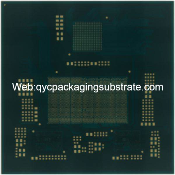
Package substrate design
The purpose of this article is to provide an in-depth look at the diversity and innovation of packaging substrate designs to reveal the key players in this field. We will demonstrate multiple aspects of packaging substrate design, including different design principles, innovative approaches, material selection, and their role in various application areas. Through this content, we will provide engineers and electronics industry practitioners with insights into how to better understand, apply and continuously innovate packaging substrate design. Whether you’re an engineer looking to solve a specific design challenge, or an SEO professional looking to learn more about the field, this article will provide you with in-depth insights and a fresh perspective, allowing you to better prepare for the ongoing evolution of the electronics industry and changes.
What is Package Substrate Design?
Package Substrate Design is a key engineering area concerned with designing and building package substrates in electronic devices to support component connections, circuit performance and overall reliability. In this area, engineers carefully consider many factors, including material selection, hardware layout, signal integrity, thermal performance, etc., to ensure the normal operation of electronic equipment.
Package substrate design plays a vital role in the electronics field. It is the nerve center of electronic devices, connecting various components and integrated circuits to enable the device to function properly. The quality and innovation of packaging substrate design directly affects the performance, reliability and cost-effectiveness of electronic devices. This field not only plays a key role in traditional electronic products such as printed circuit boards (PCBs) and chip packaging, but also plays an important role in communication technology, automotive electronic systems and other fields. Therefore, a deep understanding of packaging substrate design is critical to enable innovation, improve electronic device performance, and meet growing market demands.
Key elements and design principles
Material Selection: The Crucial Basics
In packaging substrate design, material selection is one of the decisive factors. Different materials have their own advantages and applications, ranging from common fiberglass reinforced resin (FR-4) to high-performance ceramics, which have a wide range of applications. Typically used in general applications, FR-4 is popular for its low cost and availability. However, in high frequency applications, materials such as ceramics provide better insulation and thermal conductivity properties. The key to material selection is to control costs while meeting design requirements, which requires a comprehensive consideration of the material’s thermal properties, electrical properties, and manufacturability.
Hardware and Layout: Key Drivers of Performance
Hardware and layout decisions play a critical role in package substrate design. The location, connection, and hierarchical arrangement of components directly affect circuit performance. Optimizing hardware layout can reduce signal transmission delay, reduce signal crosstalk, and improve overall performance. Additionally, sound hardware and layout decisions can reduce circuit complexity and improve maintainability, taking into account power distribution, signal integrity, and thermal requirements.
Signal integrity: ensuring accurate transmission of data
Signal integrity is a key consideration in package substrate design, especially in high-speed digital systems. This involves maintaining the accurate transmission of signals to avoid signal crashes, timing issues, and other potential electromagnetic interference. Adopting appropriate hierarchical design, noise suppression techniques, and differential signaling can help ensure signal integrity, thereby improving system reliability and performance.
Thermal and Temperature Management: Key to Performance Optimization
In high-performance electronic systems, thermal design and temperature management are critical. Thermal effects directly affect the stability and life of components. Therefore, designers must consider appropriate thermal solutions such as heat sinks, fans, heat pipes, etc. to ensure temperatures are within acceptable limits. Through effective temperature management, not only can the reliability of electronic systems be improved, but higher performance and longer service life can also be achieved.
These key elements and design principles are the foundation of package substrate design and are critical to meeting performance requirements and enabling innovation. Material selection, hardware layout, signal integrity, and thermal management all require careful consideration to ensure design success and the superiority of the final product.
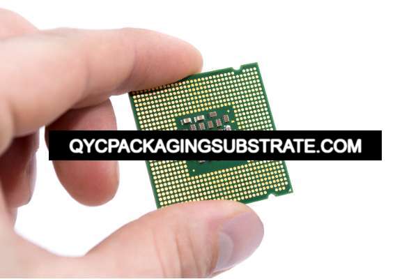
Package substrate design
Innovative design methods
3D packaging: broaden horizons and break through dimensional limitations
Advantage:3D packaging is the key to the future, providing greater functional density for electronic devices.
Improve performance:Process more data and tasks with multiple layers of vertical stacking.
Space optimization:Accommodate more components in a limited space, making the device thinner and lighter.
Thermal improvements:More effective heat dissipation path, extending equipment life.
Challenge: Obstacles to overcome when implementing 3D packaging
Thermal management:Increased component density requires more complex thermal solutions.
Manufacturing Complexity:Stacking and connecting multiple layers requires higher manufacturing techniques.
Cost:Designing and producing 3D packages requires more resources.
Flexible circuit board design: breaking rigidity and giving versatility
The Meaning of Flexibility: Why Flexible Board Design is So Important
Adaptability:Suitable for devices of all shapes and sizes.
Save space:Bending and folding circuit boards can reduce device size.
Reduce weight:Reduces the burden on rigid substrates, making devices lighter.
Versatility:One circuit board, multiple functions
Integrated components:Integrate components such as sensors and antennas directly onto the circuit board.
Flexible circuit:Supports flexibility and changeable shapes for a variety of applications.
High-density interconnect technology: new possibilities for connectivity
Improve performance:Tighter connections speed up data transfers.
Space efficiency:Reduce the space occupied by the connection.
Maintainability:Easier to repair and upgrade.
These innovative design methods provide new perspectives and technical approaches for packaging substrate design, promoting the continuous development and innovation of electronic equipment. While they meet increasingly complex electronic needs, they also bring challenges that require engineers to continuously explore and improve.
Application areas
Package substrate design plays a vital role in the field of electronic products. It is a core component of many electronic devices, ensuring strong connections between components and supporting smooth signal transmission. An obvious example is smartphones, where the packaging substrate not only connects various chips and circuits, but also implements complex multi-layer wiring to ensure high performance and miniaturization. In addition, tablets, laptops, and home electronic devices also rely on packaging substrates to provide reliable electronic connections and signal transmission.
In the field of communication technology, packaging substrate design is a key factor in ensuring the efficient operation of communication equipment. For example, packaged substrates in base station antenna control units (ACUs) support radio frequency transmission and signal processing to ensure the reliability of communication networks. In addition, packaging substrates also play a key role in network switching equipment, fiber optic communication modules and satellite communication systems. Its high-density cabling technology and signal integrity support high-speed data transmission and seamless communications, making modern communications technology possible.
Package substrate design also plays an increasingly important role in the automotive industry. As the number of automotive electronic systems continues to increase, including in-car entertainment systems, navigation systems, engine control units, etc., packaging substrates have become the core of these systems. They must be able to operate under extreme temperature and vibration conditions while maintaining reliable circuit performance. In addition, packaging substrates support vehicle communications, autonomous driving technology and vehicle safety systems. In the automotive industry, innovation in packaging substrate design is key to meet growing demands and safety standards.
These application cases highlight the diversity and critical role of packaging substrate design in the electronics, communications technology and automotive industries. They support the development of modern science and technology, enabling various fields to provide more advanced and reliable products and services.
Future trends
In the future, packaging substrate design will be deeply influenced by advanced technologies. Keywords include 5G technology, artificial intelligence, Internet of Things and quantum computing. The rise of these technologies will bring higher performance requirements and smaller package sizes. For example, widespread adoption of 5G will require higher data transmission speeds and lower latency, which will drive higher-density packaging substrate designs to meet this demand. Additionally, the proliferation of AI and IoT devices will require more compact and energy-efficient designs, which will drive innovative packaging methods, including three-dimensional packaging and more integrated circuits. In addition, the emergence of quantum computing will trigger huge changes in the field of data processing and storage, which will pose new challenges and opportunities for packaging substrate design.
As awareness of sustainability and environmental protection increases, packaging substrate design will also move in a more environmentally friendly direction. In this trend, keywords include green materials, recyclability and low-energy production. Manufacturers will increasingly focus on using renewable and degradable materials to reduce environmental impact. In addition, adopting more efficient manufacturing processes, such as low-energy processes, will help reduce energy consumption and lower carbon emissions. Sustainable design not only benefits the environment, but also helps reduce costs and make products more sustainable.
In the future, the field of packaging substrate design will need to strike a balance between technology and sustainability to meet increasingly complex needs and protect our environment. This will bring new opportunities and challenges to engineers and designers, while also driving the electronics industry towards a more sustainable and innovative future.
In conclusion
After reviewing the full text of Package Substrate Design, it is not difficult to see the key role of package substrate design in the field of modern electronics. These designs not only make our electronic devices smaller and more efficient, they also give them greater performance and reliability. Package substrate design ensures circuit stability and performance through appropriate material selection, precise hardware layout, and optimized signal integrity. In addition, temperature management and thermal design cannot be ignored as they help extend the life of the device and improve performance.
The field of packaging substrate design is filled with endless potential and opportunities, but it also comes with challenges. Continuous innovation is essential because technology is constantly evolving and user needs continue to evolve. Meeting the challenges requires addressing the introduction of new materials, new processes and new technologies, while also maintaining sustainability and environmental principles. As a result, engineers need to continually learn and adapt to remain competitive in this evolving field.
In short, Package Substrate Design plays a vital role in the electronics industry, not only promoting the advancement of technology, but also bringing more convenience to our lives and work. Through continuous innovation, we can realize its full potential, meet the challenges of the future, and achieve better design and performance.