 Professional Flip-Chip Packaging Substrate Supplier

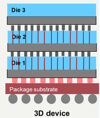
What is 3D IC Package Substrate?
3D IC Package Firm and 3D IC Package Substrate Supplier, we mainly produce ultra-small bump pitch substrate, ultra-small trace and 3D IC Package Service.
3D IC Package Substrate is a key electronic component that plays an important role in the modern electronics field. In short, 3D IC Package Substrate is a substrate for three-dimensional integrated circuit packaging that provides a platform to support and connect electronic devices.
In modern electronic devices, 3D IC Package Substrate plays a key role in connecting and supporting electronic components. It not only provides physical support for electronic devices, but also connects the signal transmission paths between various devices through its complex wiring structure. This structure makes communication between electronic devices more efficient while reducing the system’s footprint and improving overall performance and efficiency.
3D IC Package Substrate does much more than that. In the field of modern electronics, especially in the fields of high-performance computing, artificial intelligence and communication technology, there is an increasingly urgent need for higher integration and faster data transmission speeds. The 3D IC Package Substrate can exactly meet these needs. By stacking multiple layers of devices in the vertical direction, 3D IC Package Substrate can achieve higher device density and shorter signal transmission paths, thereby improving the overall performance and response speed of the system.
In short, 3D IC Package Substrate is an indispensable part of the modern electronics field. By providing a platform to support and connect electronic devices, it enables efficient communication and collaborative work between electronic devices, and promotes the continuous development and progress of electronic technology. In the future, as electronic devices become further intelligent and functional, 3D IC Package Substrate will continue to play a vital role, injecting new vitality and power into innovation and development in the electronic field.
What are the advantages of 3D IC Package Substrate?
In the field of modern electronics, 3D IC Package Substrate, as an advanced packaging technology, has obvious advantages over traditional packaging methods. Here are its main advantages:
3D IC Package Substrate uses vertical stacking of multi-layer chips to make the connections between chips closer and shorten the signal transmission path, thereby significantly improving the performance of electronic devices. In this way, not only can higher processing speed and lower power consumption be achieved, but the overall performance of the system can also be improved.
Compared with traditional horizontal wiring methods, 3D IC Package Substrate greatly improves the space utilization efficiency of the system by vertically stacking multi-layer chips. This vertically integrated design can effectively reduce the footprint of the system board, making the electronic equipment more compact in size, while improving the integration and density of the system.
Because 3D IC Package Substrate can implement more functions in a smaller space, it can reduce the distance between components in the system, thereby reducing energy transmission losses. This means that electronic devices consume less energy when running, helping to improve the device’s energy efficiency ratio, extend battery life, and reduce reliance on cooling systems.
3D IC Package Substrate integrates multiple functional components into one package, which not only simplifies the design and layout of the circuit board, but also improves the integration of the system. This integrated design makes electronic equipment lighter and more compact, while reducing assembly costs and production cycles, facilitating the rapid development of electronic products.
Due to the high degree of integration and superior performance of 3D IC Package Substrate, it provides unlimited possibilities for innovative development in the electronic field. By integrating multiple functional modules into one package, more types of applications can be realized, thus promoting innovation and applications in artificial intelligence, Internet of Things, smart wear and other fields.
In general, 3D IC Package Substrate has obvious advantages over traditional packaging methods, including improving performance, improving space efficiency, reducing energy consumption, improving system integration and promoting innovative development. With the continuous advancement of technology and the expansion of application scope, I believe it will play an increasingly important role in the future electronic field.
Why choose 3D IC Package Substrate?
When designing and manufacturing electronic devices, why should we choose 3D IC Package Substrate instead of other packaging methods? This question is critical because the correct choice of packaging method has a direct impact on the performance, stability and reliability of electronic devices. Some key factors will be explored below to better understand why 3D IC Package Substrate was chosen.
First, 3D IC Package Substrate has excellent performance characteristics. Compared with traditional packaging methods, such as surface mount technology (SMT) or chip packaging technology (CSP), 3D IC Package Substrate can achieve higher integration and faster data transmission speeds. By stacking multi-layer devices in the vertical direction, 3D IC Package Substrate can greatly reduce the space occupied by the circuit board and improve signal transmission efficiency, thus providing a significant improvement in the performance of the device.
Secondly, 3D IC Package Substrate has higher reliability and stability. Due to the stacked structure of the device, 3D IC Package Substrate can reduce the number of connection points on the circuit board, thereby reducing the possibility of failure. In addition, by using advanced packaging materials and process technology, 3D IC Package Substrate can also improve the high temperature resistance and vibration resistance of electronic equipment, ensuring that the equipment can operate stably under various environmental conditions.
Finally, there are many successful cases that prove the superior performance of 3D IC Package Substrate. For example, in the field of high-performance computing, 3D IC Package Substrate has been widely used in the packaging of key components such as processors and graphics cards, providing powerful computing capabilities for supercomputers and data centers. In the field of mobile devices, 3D IC Package Substrate is also used in the packaging of devices such as smartphones and tablets, providing users with a faster and more stable experience.
To sum up, choosing 3D IC Package Substrate instead of other packaging methods can provide electronic devices with higher performance, better stability and broader application prospects. By making full use of the advantages of 3D IC Package Substrate, we can better meet the needs of users and promote the development of electronic technology to new heights.
What is the manufacturing process of 3D IC Package Substrate?
The manufacturing process of 3D IC Package Substrate is a precise and complex project involving multiple steps and key technologies. Below we will delve into this process, including the steps to manufacture a 3D IC Package Substrate and the differences between motherboard and substrate manufacturing.
Design and Planning: The first step in manufacturing a 3D IC Package Substrate is design and planning. This includes determining circuit layout, connections, and hierarchy. Design teams must consider factors such as circuit complexity, signal transmission efficiency, and thermal requirements.
Material Preparation: During the manufacturing process, choosing the right materials is crucial. Commonly used materials include dielectrics, metal wires, insulation layers, etc. These materials must have good electrical conductivity, thermal conductivity and mechanical properties to ensure the stability and reliability of the 3D IC Package Substrate.
Molding and lamination: Next, the prepared materials are molded and laminated according to the design requirements. The process involves stacking different layers of material together and using heat and pressure to bond them into a whole. This ensures that the circuit is firmly connected and layered.
Processing and manufacturing: Manufacturing 3D IC Package Substrate requires precision processing and manufacturing. This includes the use of photolithography, etching, and metal deposition technologies to finely process the circuit to ensure its accuracy and reliability.
Motherboard manufacturing: The motherboard is the core component that supports the entire electronic system and is usually made of materials such as fiberglass reinforced epoxy resin (FR-4). The key steps in motherboard manufacturing include: pre-processing, drilling, etching, plating and final inspection and testing. The focus of motherboard manufacturing is to ensure that the geometric dimensions and electrical characteristics of the circuit board meet the design requirements.
Substrate manufacturing: Substrate is the core component of 3D IC Package Substrate and is used to connect different chips and components. Key steps in substrate manufacturing include: lamination, hole coppering, board preparation, patterning, drilling and final inspection and testing. Compared with motherboards, the manufacturing of substrates is more complex and requires higher precision and more process steps.
Through the above manufacturing process, we can see that manufacturing 3D IC Package Substrate requires highly precise processes and advanced technology. The manufacturing processes of motherboards and substrates are different, but together they form a key component of 3D IC Package Substrate, providing a solid foundation for the implementation of advanced electronic systems.
3D IC Package Substrate
In what fields is 3D IC Package Substrate applied?
As a key technology, 3D IC Package Substrate has been widely used in many fields, including high-performance computing and artificial intelligence. Let’s take a closer look at its role in these areas.
High-performance computing is a field that requires processing large-scale data and complex computing tasks. In this area, 3D IC Package Substrate plays an important role. First of all, it can realize multi-chip stacking and improve data transmission speed and processing efficiency by increasing the communication bandwidth between chips. Secondly, 3D IC Package Substrate can also achieve high-density integration and integrate multiple functional modules into a small package, thereby improving system performance and power consumption efficiency. Therefore, in the field of high-performance computing, 3D IC Package Substrate is widely used to build key equipment such as supercomputers and data center servers, providing strong support for tasks such as scientific computing, weather forecasting, and medical image processing.
Artificial intelligence is a field that has developed rapidly in recent years, and the demand for computing resources is also increasing. In artificial intelligence applications, 3D IC Package Substrate plays a vital role. First, it can achieve a high degree of integration, integrating multiple functions such as sensors, processors, and memories into a small package, thereby improving the system’s integration and performance density. Secondly, 3D IC Package Substrate can also achieve heterogeneous integration, integrating different types of chips (such as CPU, GPU, FPGA, etc.) into the same package, thereby achieving a more flexible system architecture and higher computing efficiency. Therefore, in the field of artificial intelligence, 3D IC Package Substrate is widely used to build smart devices such as smartphones, smart cameras, and self-driving cars, providing strong support for the development of artificial intelligence technology.
In summary, 3D IC Package Substrate has important application value in fields such as high-performance computing and artificial intelligence. It can not only improve system performance and power consumption efficiency, but also achieve a more flexible system architecture and higher computing efficiency. It has brought new opportunities and challenges to the development of related industries.
How to obtain 3D IC Package Substrate?
To obtain a reliable 3D IC Package Substrate supplier and make an informed choice, there are a number of key factors to consider. Here are some guidelines to help ensure you choose a supplier that meets your needs and provides high-quality products and services.
Before choosing a supplier, learn about reliable 3D IC Package Substrate suppliers through market research and industry surveys. Review customer reviews, industry reports, and credibility ratings to determine which vendors have a good reputation in the market and have reliable production capabilities and product quality.
Look for suppliers with extensive experience and expertise, especially in the field of 3D IC Package Substrate. They should understand industry standards, technology trends, and the latest manufacturing methods to ensure they can meet your technical requirements and quality standards.
Make sure the supplier you choose offers certified, high-quality products. Check their quality management systems and production processes to ensure compliance with relevant international standards and industry regulations. This ensures that the 3D IC Package Substrate you get meets your performance and reliability requirements.
Understand the supplier’s manufacturing capabilities and supply chain management capabilities. They should have advanced manufacturing equipment and production processes to ensure timely delivery of high-quality products. In addition, their supply chain management should be sound and able to deal with potential supply risks and ensure the stability of supply.
Choose a supplier that provides excellent customer service and technical support. They should be able to respond to your inquiries and needs in a timely manner and provide professional technical support to help you solve problems and challenges that may arise.
Consider the supplier’s price competitiveness and cooperation conditions. Make sure their quote is reasonable and matches your budget and project requirements. At the same time, understand their terms and conditions of cooperation to ensure that a good cooperative relationship can be established and the interests of both parties can be maximized.
When selecting a supplier, taking the above factors into consideration and establishing a close cooperative relationship with the supplier can help you obtain a high-quality, reliable 3D IC Package Substrate and achieve successful implementation and sustainable development of the project.
What is the quote for 3D IC Package Substrate?
Before looking at the price of 3D IC Package Substrate, we need to consider several key factors. First of all, the price of 3D IC Package Substrate is affected by multiple factors, including but not limited to material cost, manufacturing process complexity, level of technological innovation, and market demand. Secondly, obtaining an accurate quote requires communicating with the supplier and taking into account factors such as required specifications, quantity, delivery time, etc.
The price of 3D IC Package Substrate is affected by multiple factors. First, material cost is an important factor, and different types of substrate material prices may vary. Secondly, the complexity of the manufacturing process will also directly affect the price, because more advanced manufacturing processes usually require higher costs. In addition, the degree of technological innovation is also one of the factors that affects the price. The new 3D IC Package Substrate technology may bring additional costs. Finally, market demand will also have an impact on prices, and imbalances in supply and demand may lead to price fluctuations.
To obtain an accurate quote for 3D IC Package Substrate, it is best to contact the supplier directly. By communicating with multiple suppliers, you can compare quotes and services from different companies and choose the one that best suits your needs. When communicating with suppliers, clear product specifications, quantities, delivery time and other information need to be provided so that suppliers can give accurate quotations.
When choosing a 3D IC Package Substrate supplier, in addition to price, you also need to consider cost-effectiveness. Cost-effectiveness not only includes price factors, but also considers the supplier’s technical capabilities, product quality, delivery time, after-sales service, etc. A high-quality supplier should not only provide reasonable prices, but also have good technical support and after-sales service to ensure that customers receive satisfactory products and services.
To sum up, the quotation of 3D IC Package Substrate is affected by many factors. Obtaining an accurate quotation requires communication with suppliers, and comprehensive consideration of factors such as price, technical capabilities, product quality, etc., to choose the supplier that best suits your needs.
What are the frequently asked questions about 3D IC Package Substrate?
What are the common challenges in manufacturing 3D IC Package Substrates?
Manufacturing 3D IC Package Substrates involves intricate processes, including bonding, thinning, and interconnecting multiple layers. Common challenges include maintaining uniformity across layers, controlling thermal expansion, and ensuring reliability in high-density interconnections.
What are the thermal management considerations for 3D IC Package Substrates?
Thermal management is crucial due to the compact nature of 3D ICs. Issues such as heat dissipation, thermal conductivity of substrate materials, and thermal stress at bonding interfaces need careful consideration to prevent performance degradation and reliability issues.
How do design constraints impact 3D IC Package Substrate implementation?
Design constraints, such as signal integrity, power integrity, and thermal constraints, significantly influence the layout and architecture of 3D IC Package Substrates. Balancing these constraints while optimizing performance poses a challenge for designers.
What are the reliability concerns associated with 3D IC Package Substrates?
Reliability concerns include interconnect reliability, solder joint reliability, and the impact of thermal cycling on the substrate and integrated circuits. Ensuring long-term reliability under varying operating conditions is essential for the success of 3D ICs.
How does the cost of 3D IC Package Substrate compare to traditional packaging methods?
3D IC Package Substrate typically incurs higher manufacturing costs due to the complexity of fabrication processes and the use of advanced materials. However, the benefits in terms of performance, miniaturization, and integration often justify the investment.