 Professional Flip-Chip Packaging Substrate Supplier

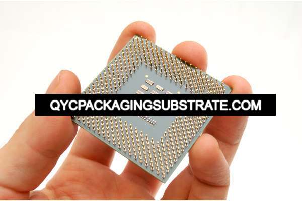
ABF GZ41R2H Package Substrates Manufacturer , we mainly produce ultra-small bump pitch substrate, ultra-small trace and spacing packaging substrate and PCBs.
With the continuous advancement of technology, electronic products are becoming more and more complex, and the development of PCB (Printed Circuit Board) technology is an important driving force for this progress. In modern electronic equipment, ABF GZ41R2H packaging substrate, as a key component, is bringing revolutionary changes to the electronics industry. ABF GZ41R2H packaging substrate not only provides excellent electrical performance and reliability, but also provides new possibilities for the design and manufacturing of various high-end electronic products. Its advanced materials and manufacturing processes make it an indispensable part of today’s electronics industry, leading the new trend of electronic technology.
What are ABF GZ41R2H Package Substrates?
ABF GZ41R2H packaging substrate is an advanced PCB technology that represents the latest development trend in the electronics industry. As a key component of modern electronics, it not only delivers outstanding performance but also exhibits unparalleled reliability. One of its core advantages is the use of high-performance ABF (Ajinomoto Build-up Film) material, which not only has excellent thermal conductivity and electrical properties, but also has good mechanical strength and can withstand challenges in various environments.
ABF GZ41R2H Package Substrates Manufacturer
The design and process of the ABF GZ41R2H packaging substrate are also its outstanding features. With the help of advanced manufacturing technology and precise process flow, each packaging substrate undergoes strict quality control and inspection to ensure that its performance is stable and reliable. This comprehensive combination of high-performance materials, advanced processes and exquisite design enables the ABF GZ41R2H packaging substrate to provide excellent electrical characteristics and mechanical strength for a variety of electronic products.
Whether used in small smartphones or large industrial control systems, the ABF GZ41R2H packaging substrate can meet the needs of various application scenarios. Its flexible size design and customizable features make it one of the first choices in the electronics industry. Whether in the fields of consumer electronics, communications, medical or aerospace, ABF GZ41R2H packaging substrate has demonstrated its irreplaceable value.
Overall, the ABF GZ41R2H packaging substrate represents the latest development direction of PCB technology, and its excellent performance and reliability will bring new possibilities to the design and manufacturing of electronic products. With the continuous advancement of technology, I believe that the ABF GZ41R2H packaging substrate will continue to play an important role in promoting the electronics industry towards a better future.
ABF GZ41R2H Package Substrates design Reference Guide.
ABF GZ41R2H package substrate is an advanced PCB technology that provides new possibilities for the design and manufacturing of electronic devices. When designing the ABF GZ41R2H package substrate, a number of key factors need to be considered to ensure the highest level of performance and reliability of the final product. The following is a design reference guide to help engineers better understand and apply ABF GZ41R2H package substrate technology:
Material selection
When designing the ABF GZ41R2H package substrate, proper material selection is critical. High-quality ABF material and copper foil can ensure good electrical characteristics and stable signal transmission.
Hierarchical design
Considering the complexity of electronic devices, the hierarchical structure of the packaging substrate should be properly planned during design. By properly allocating signal, power, and ground layers, signal interference and electromagnetic interference can be minimized.
Interface design
The interface design of the ABF GZ41R2H package substrate should take into account how the device is connected to external components. Reasonable layout of interface locations and taking appropriate protective measures can effectively protect interfaces from mechanical damage and environmental impacts.
Thermal design
For high-power electronic equipment, good thermal design is crucial. When designing the ABF GZ41R2H package substrate, the heat sink layout and thermal path should be taken into consideration to ensure that the device can effectively dissipate heat when operating at high load for a long time.
Environmental adaptability
The ABF GZ41R2H packaging substrate should have good environmental adaptability and be able to work stably under various temperature, humidity and vibration conditions. Environmental factors should be taken into consideration during design and appropriate protective measures and packaging materials should be selected.
Production manufacturability
Finally, the feasibility of manufacturing should be taken into consideration when designing. Properly designing the structure and layout of the packaging substrate can reduce production costs and improve production efficiency.
To sum up, designing the ABF GZ41R2H package substrate requires comprehensive consideration of factors such as material selection, layer design, interface design, heat dissipation design, environmental adaptability and production manufacturability. Through reasonable design and strict manufacturing processes, we can ensure that the final product has excellent performance and reliability and meets the needs of various application scenarios.
What material is used in ABF GZ41R2H Package Substrates?
ABF GZ41R2H packaging substrate is a highly respected advanced technology in today’s electronics industry. Its material selection is the cornerstone of its exceptional performance. This packaging substrate uses high-quality ABF (Ajinomoto Build-up Film) material, which has excellent thermal conductivity and electrical properties. ABF material is a multi-layer thin film structure that is processed through a special process to achieve efficient signal transmission and thermal management while maintaining a high degree of stability. This means that in high-density circuit designs, the ABF GZ41R2H package substrate can ensure reliable connections between circuits while effectively dissipating heat to maintain stable system operation.
In addition to ABF materials, the ABF GZ41R2H package substrate also uses high-quality copper foil as the conductive layer. The use of copper foil as a conductive layer ensures the stability and reliability of the circuit. Copper has good electrical and thermal conductivity and can effectively transmit signals and dissipate heat, thus ensuring high-performance operation of the circuit. Combined with the ABF material, the copper foil provides a stable electrical connection and signal transmission to the ABF GZ41R2H package substrate. This means that in various application scenarios, the ABF GZ41R2H package substrate can maintain excellent performance and ensure system reliability and stability.
In short, the material selection of the ABF GZ41R2H package substrate is an important guarantee for its excellent performance. By using high-quality ABF materials and high-quality copper foil, this packaging substrate can perform well in various application scenarios, providing a reliable foundation for the design and manufacturing of electronic products.
What size are ABF GZ41R2H Package Substrates?
The size of the ABF GZ41R2H package substrate is an important design consideration as it needs to accommodate the varying needs of various electronic devices. This packaging substrate can be customized to meet the requirements of specific applications to accommodate a variety of sizes and shapes. Whether it is a small smartphone or a large industrial control system, the ABF GZ41R2H package substrate can provide stable and reliable circuit connections and excellent performance.
In small devices such as smartphones, the size of the packaging substrate is usually very compact, requiring space utilization efficiency and tight arrangement of components to be considered. The ABF GZ41R2H package substrate can be designed to be very thin and highly integrated to ensure complex circuit layouts within limited space. At the same time, its excellent thermal conductivity can also effectively help control the temperature of electronic equipment and improve the overall performance stability.
In applications such as large industrial control systems, packaging substrates usually require larger sizes to accommodate more electronic components and connection interfaces. ABF GZ41R2H package substrates can be designed into various sizes and shapes according to system requirements to meet the layout needs of complex systems. Its excellent mechanical strength and electrical characteristics allow it to maintain stable and reliable performance in harsh working environments, providing reliable circuit support for applications such as industrial control systems.
Overall, the size customization capabilities of the ABF GZ41R2H package substrate provide flexibility and convenience in the design and manufacturing of a variety of electronic devices. Whether it is a small smartphone or a large industrial control system, this advanced packaging substrate technology can be used to achieve efficient and stable circuit connections and promote the sustainable development of the electronics industry.
The Manufacturer Process of ABF GZ41R2H Package Substrates.
The manufacturing process of the ABF GZ41R2H package substrate is a precise and complex process that is carefully designed and strictly controlled to ensure the highest standards of quality and performance for each package substrate. The manufacturing process includes the following key steps:
Design phase
In the early stages of the manufacturing process, a team of engineers uses advanced design software to design circuit board layouts and connection plans that meet specifications based on customer requirements and application needs. At this stage, taking into account the complexity and performance requirements of the circuit, careful planning and analysis is required to ensure the functionality and stability of the final product.
Printing
Next, the designed circuit board layout is transferred to the substrate material. This is usually done by converting the design file into a format that can be read by a printer and using screen printing technology to print a conductive material (such as copper) onto the surface of the substrate. The accuracy and precision of this step are critical to the subsequent manufacturing process.
Etching
Once the conductive material is printed on the substrate, the etching process follows. Etching is the process of removing unwanted portions of material from a substrate to form the circuit board’s outlines and conductor routes. This is usually accomplished by dipping the substrate into a chemical solution that dissolves away the portion of the material that is not being printed.
Assemble
After etching is complete, the substrate will enter the assembly stage. At this stage, the components on the circuit board (such as resistors, capacitors, integrated circuits, etc.) will be accurately installed in the designed positions and connected to wires through techniques such as soldering. The assembly process requires a high degree of precision and technical skill to ensure that each element is installed correctly and connected well.
Inspection and testing
Finally, the manufactured packaging substrate will undergo rigorous inspection and testing. This includes visual inspection, functional testing, electrical performance testing, etc. to ensure that the quality and performance of the circuit board meet the design requirements. Any products that do not meet the standards will be eliminated to ensure that the final products delivered to customers are reliable and of high quality.
To sum up, the manufacturing process of ABF GZ41R2H packaging substrate is a highly precise and complex process that requires strict control and careful design. Through the precise execution of each key step, we ensure that each packaging substrate can meet the highest quality standards and provide customers with reliable and high-performance electronic products.
The Application area of ABF GZ41R2H Package Substrates.
As a high-performance PCB technology, ABF GZ41R2H packaging substrate is widely used in multiple industries, providing reliable circuit connections and stable performance for various electronic products. The following are its applications in consumer electronics, communications, medical and aerospace:
In the field of consumer electronics, ABF GZ41R2H packaging substrates are widely used in various products such as smartphones, tablets, and smart home devices. Its high performance and reliability ensure the stable operation of the equipment, while meeting consumer demands for electronic product performance and durability. Whether it is a high-definition display, a complex sensor system or fast data transmission, the ABF GZ41R2H packaging substrate can provide reliable support, making consumer electronics more intelligent and convenient.
In the field of communications, ABF GZ41R2H packaging substrates are used to manufacture various communications equipment, such as base stations, routers, optical fiber communications equipment, etc. These devices have extremely high requirements for high-speed data transmission, stable signal transmission and long-term operation reliability, and the ABF GZ41R2H packaging substrate can meet these requirements, ensure the stability and reliability of the communication network, and promote the development and development of the information society. Advances in communication technology.
In the medical field, ABF GZ41R2H packaging substrates are used to manufacture various medical equipment, such as medical imaging equipment, heart monitors, implantable medical devices, etc. These devices have extremely high requirements for the accuracy and reliability of data collection, processing and transmission. They must also be able to adapt to the special requirements of the medical environment, such as anti-interference and high temperature resistance. The high performance and reliability of the ABF GZ41R2H packaging substrate enable these medical devices to accurately monitor and diagnose diseases, provide accurate data support for medical staff, and ensure the health and safety of patients.
In the aerospace field, ABF GZ41R2H packaging substrates are used in the manufacturing of aerospace devices and aerospace devices. The aerospace field has extremely high requirements for the reliability and stability of electronic products. Through its excellent electrical characteristics and mechanical strength, the ABF GZ41R2H packaging substrate provides reliable circuit connections and stable performance for aerospace devices, ensuring aerospace missions. smooth and safe operation.
In general, ABF GZ41R2H packaging substrate plays an important role in applications in many fields, providing stable and reliable circuit connections and performance support for various electronic products, and promoting technological development and innovation in various industries.
What are the advantages of ABF GZ41R2H Package Substrates?
ABF GZ41R2H packaging substrate is a breakthrough technology in today’s electronic field. Compared with traditional PCB technology, it shows many advantages and brings new possibilities to the design and manufacturing of electronic products.
First, the ABF GZ41R2H package substrate offers higher performance. Using advanced ABF materials and processes, the packaging substrate has excellent electrical characteristics, signal transmission speed and anti-interference ability, and can meet the growing performance requirements of electronic products. Whether it is a high-frequency application or a low-power design, the ABF GZ41R2H package substrate can provide excellent performance.
Secondly, the ABF GZ41R2H package substrate has a more reliable connection. Through precise manufacturing processes and high-quality material selection, the packaging substrate can ensure stable electrical connection and mechanical strength, reduce the risk of failure caused by connection problems, and improve product reliability and stability.
In addition, the ABF GZ41R2H package substrate has a longer service life. Excellent materials and processes ensure the durability and anti-aging capabilities of the packaging substrate. It can maintain stable performance in various harsh environments, extend the service life of electronic products, and reduce maintenance costs.
Finally, the ABF GZ41R2H package substrate offers a higher level of integration. Its advanced design and manufacturing technology enables the packaging substrate to achieve higher device density and more complex circuit layout, thereby reducing the size of electronic products and enhancing functionality, providing product designers with more space and flexibility sex.
In short, the many advantages of the ABF GZ41R2H packaging substrate, including high performance, reliable connection, long life and high integration, open up new prospects for the design and manufacturing of electronic products and will inject strong impetus into future technological development and innovation.
FAQ
How does the ABF GZ41R2H package substrate differ from traditional PCB technology?
The ABF GZ41R2H package substrate uses advanced ABF materials and processes and has several key differences compared to traditional PCB technology. First, the ABF GZ41R2H package substrate uses high-performance ABF material, which has better thermal conductivity and electrical properties, thereby improving the performance and stability of the entire system. Secondly, the manufacturing process uses advanced production technology, including precision design, printing, etching and assembly processes to ensure that the quality and performance of each packaging substrate can meet the highest standards. In addition, the ABF GZ41R2H packaging substrate also has higher integration and more reliable connections, making it widely used in various high-end electronic products.
What fields is ABF GZ41R2H packaging substrate suitable for?
ABF GZ41R2H packaging substrate is suitable for various fields, including consumer electronics, communications, medical, aerospace, etc. In the field of consumer electronics, it can be used in the manufacturing of smartphones, tablets, home appliances and other products; in the field of communications, it can be used in the manufacturing of base station equipment, communication network equipment, etc.; in the medical field, it can be used in medical equipment , manufacturing of diagnostic instruments, etc.; in the aerospace field, it can be used in the manufacturing of aircraft, satellites, etc. In summary, ABF GZ41R2H packaging substrate provides reliable circuit connections and stable performance for products in various industries and is a key component of modern electronic product manufacturing.
What is the manufacturing process of ABF GZ41R2H package substrate?
The manufacturing process of the ABF GZ41R2H package substrate is carefully designed and strictly controlled, including critical steps such as design, printing, etching and assembly. First, according to the design requirements of the product, the packaging substrate is designed and the circuit connections and layout are determined. Then, advanced printing technology is used to print circuit patterns and other necessary marks on the substrate. Next, through an etching process, the unwanted portions of material are removed, leaving the desired lines and connection points. Finally, assembly and testing are performed to ensure that the quality and performance of each package substrate meet the requirements. This process requires sophisticated equipment and technical support to ensure the production of high-quality packaging substrates.