 Professional Flip-Chip Packaging Substrate Supplier

Advanced Semiconductor Glass Substrates manufacturer, we have made 14 layers FC BGA package substrates. we also can produce the Advanced Glass Substrates,The glass substrate is more resistant to high temperatures and is more flat.
In the field of modern electronics, Advanced Semiconductor Glass Substrates are an indispensable key component in electronic equipment. These substrates provide solid support and reliable electrical connections to electronic devices while providing excellent thermal properties and mechanical strength. A thorough understanding of the definition, design, manufacturing processes, and associated costs and materials of advanced semiconductor glass substrates is critical for electronics engineers and hobbyists.
What is an advanced semiconductor glass substrate?
Advanced Semiconductor Glass Substrates are a key technology in today’s semiconductor industry, providing a solid foundation for the performance and reliability of electronic devices. These substrates serve as carriers for semiconductor devices, carrying electronic components and providing the necessary electrical connections. Compared with traditional substrate materials, advanced semiconductor glass substrates have a series of unique advantages, making them an indispensable part of modern electronic devices.
First, advanced semiconductor glass substrates have excellent thermal properties. In high-temperature environments, traditional substrate materials may deform or expand thermally, affecting the stability and performance of electronic components. Advanced semiconductor glass substrates can remain stable over a wide temperature range, ensuring the normal operation of electronic devices.
Secondly, this substrate material also has excellent mechanical strength. Since electronic devices may be affected by external forces such as vibration and impact during use, the substrate needs to have sufficient strength to protect the internal electronic components from damage. The advanced semiconductor glass substrate has high strength and wear resistance, which can effectively resist the influence of the external environment and ensure the reliability and durability of the equipment.
In addition to this, advanced semiconductor glass substrates provide a flat surface that facilitates the layout and connection of electronic components. During the circuit design process, component placement is critical to circuit performance. The flatness of the substrate ensures accurate spacing and location between components, helping to optimize circuit layout and maximize device performance.
Overall, advanced semiconductor glass substrates are one of the indispensable key components in modern electronic devices. Its excellent thermal properties, mechanical strength and flat surface provide reliable support for the stable operation of electronic devices and promote the continuous development and innovation of the semiconductor industry. With the continuous advancement of technology and the expansion of application fields, advanced semiconductor glass substrates will continue to play an important role, providing strong support for the performance improvement and functional expansion of electronic equipment.
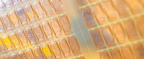
Glass Substrates
How to design advanced semiconductor glass substrates?
Designing advanced semiconductor glass substrates is a complex and delicate process that requires engineers to use specialized software and deep expertise. The following are key steps in the design process:
First, the design process begins with the capture of a circuit schematic. Engineers need to accurately understand the circuit’s functional and performance requirements and translate them into an achievable physical layout. This requires a deep understanding of the function, connections, and layout of each component in the circuit.
Next is the component layout stage. At this stage, engineers determine the location of individual electronic components on the substrate. This needs to take into account factors such as the circuit’s functional requirements, signal transmission paths, and heat distribution. Through reasonable component layout, space utilization can be optimized to the maximum extent and the stability and reliability of the circuit can be ensured.
Routing is one of the critical steps in the design process. At this stage, engineers design and lay out the connections between electronic components. This includes deciding on the path, width, and hierarchy of wires, as well as determining how signal and power lines are separated. Through carefully designed wiring, signal interference and electromagnetic interference can be minimized and the performance and stability of the circuit can be improved.
Finally, optimization of the physical layout is a critical part of the design process. Engineers need to optimize the physical layout by taking into account factors such as circuit functionality, space utilization, and manufacturability. This may involve adjusting component locations and routing paths to meet design requirements and minimize the manufacturing process.
Through these steps, engineers can transform circuit schematics into advanced semiconductor glass substrate designs that are functional, compact, and easy to manufacture. Such a design can not only meet the performance requirements of the circuit, but also maximize space utilization and reduce manufacturing costs, providing strong support for the performance and reliability of electronic equipment.
What is the manufacturing process for advanced semiconductor glass substrates?
The manufacturing process of advanced semiconductor glass substrates is a complex and precise process involving multiple key steps. Each step is crucial and directly affects the quality and performance of the final product.
First, the manufacturing process begins with substrate selection. At this stage, the manufacturer carefully selects the glass substrate suitable for the specific application. These substrates must meet strict quality standards to ensure the stability and reliability of the final product.
Next comes lamination, which is layering multiple layers of material on top of each other. These materials include glass substrates, conductive layers, and insulating layers. The lamination process requires highly precise control to ensure that the position and thickness of each layer meet design requirements.
Copper patterning is one of the key steps in the manufacturing process. At this stage, a conductive pattern is formed on the surface of the glass substrate through methods such as chemical etching or mechanical processing. These patterns will be used to connect electronic components to build circuits.
Then comes drilling. At this stage, holes are drilled into the glass substrate using techniques such as mechanical drilling or laser drilling to create electrical connections between the different layers. The location and size of the drilled holes must be precisely controlled to ensure proper operation of the circuit.
Plating is the next critical step and involves plating a layer of protective metal over the copper pattern. This protects the copper from oxidation or corrosion and provides a good soldering surface for attaching electronic components to the substrate.
Finally, there’s etching. At this stage, using chemical solutions or laser technology, unwanted metal is etched away from the substrate surface, leaving the desired conductive pattern. This process requires highly precise control to ensure the accuracy and consistency of etching.
Through the above key steps, the manufacturing process of advanced semiconductor glass substrate is completed. The final product has excellent electrical and mechanical properties and can be widely used in various electronic devices, providing solid support for the development of modern technology.
How to manufacture advanced semiconductor glass substrates?
Manufacturing advanced semiconductor glass substrates is a challenging process that requires rigorous processes and a high degree of expertise. The key steps of the manufacturing process are described below:
The first step in manufacturing advanced semiconductor glass substrates is preliminary design and preparation. This stage involves determining the specifications and requirements of the substrate, including size, number of layers, materials, etc. Designers use specialized software to convert circuit schematics into physical layouts, taking into account circuit functionality, space utilization, and manufacturing feasibility.
Once the design is complete, the substrate needs to be prepared. At this stage, engineers select the appropriate glass substrate material and perform cleaning and surface treatment to ensure the flatness and surface quality of the substrate.
Copper is one of the key materials in semiconductor glass substrates, where it is used to form conductive lines. During the copper layer deposition process, the substrate is placed in a solution containing copper ions. Through chemical reaction or electrochemical deposition, copper is deposited onto the surface of the substrate to form a conductive layer.
Wiring is the process of connecting conductive layers into a circuit. Engineers use photolithography technology to transfer the designed circuit pattern to the surface of the copper layer, and then remove the excess copper through etching or chemical processing, leaving the designed conductive lines.
The final stage of the manufacturing process is final inspection. At this stage, engineers will rigorously inspect and test the manufactured semiconductor glass substrate to ensure that it meets specifications and quality requirements. This includes checking the continuity of conductive lines, detecting possible defects or blemishes, etc.
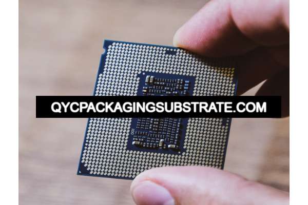
Advanced Semiconductor Glass Substrates
Manufacturing advanced semiconductor glass substrates is a precise and complex process that requires a high degree of expertise and technical capabilities from engineers. Through strict process control and quality management, the quality and reliability of the final product can be guaranteed to meet the demand for high-performance semiconductor devices in different fields.
How much do advanced semiconductor glass substrates cost?
The cost of advanced semiconductor glass substrates is one of the most critical factors in the design and manufacturing of electronic products. Understanding these cost factors is critical to developing a budget, assessing production feasibility, and ensuring project success. The following are key factors affecting the cost of advanced semiconductor glass substrates:
The size and complexity of advanced semiconductor glass substrates directly affect production costs. Larger substrate sizes typically require more material and may require longer processing times. Additionally, designs with high complexity may require more layers and subtle circuit layouts, increasing the difficulty and cost of the manufacturing process.
Substrate material is a key factor affecting cost. Different types of glass substrate materials have different properties and costs. For example, high-temperature ceramic substrates are generally more expensive than ordinary glass substrates, but have better performance in high-temperature environments. Choosing the right materials can minimize costs while meeting design requirements.
Production quantities are critical in determining the cost of advanced semiconductor glass substrates. Typically, high-volume production achieves economies of scale because fixed costs can be spread over more units of product. In contrast, low-volume production may result in higher unit costs.
Some advanced technology requirements may increase production costs. For example, if a design requires special production processes or equipment, the associated technology investments will increase manufacturing costs. Likewise, for certain applications, such as high-frequency circuits or high-density integrated circuits, higher precision and stricter quality control standards are required, which also increases costs.
Manufacturing location also affects the cost of advanced semiconductor glass substrates. In some areas, production costs may be lower because labor costs and equipment costs are relatively low. In other regions, such as developed countries, costs may be higher.
In summary, the cost of advanced semiconductor glass substrates is affected by multiple factors, including size, complexity, materials, quantity, technical requirements and manufacturing location. Understanding these factors and taking them into consideration during the design and manufacturing process can help companies develop reasonable budgets, optimize production expenses, and ensure the competitiveness and sustainability of products.
What materials are advanced semiconductor glass substrates made of?
Advanced Semiconductor Glass Substrates (Advanced Semiconductor Glass Substrates) are the core components of modern electronic equipment, and their material composition is crucial. Typically, advanced semiconductor glass substrates are composed of several key materials that together ensure the performance and reliability of the substrate.
First of all, glass substrate is one of the basic materials that constitute advanced semiconductor glass substrates. This glass substrate typically has excellent thermal properties and mechanical strength, providing a flat surface to support the layout and connection of electronic components. Selecting the appropriate glass substrate is critical to the performance of the substrate as it directly affects the thermal conductivity, mechanical strength and stability of the substrate.
Second, conductive copper wire is another key material in advanced semiconductor glass substrates. Conductive copper wire is used to form the wires and pads of circuits, making up the connections between electronic components. High-quality conductive copper wire can provide good conductivity and reliable connection, ensuring the stability and performance of the circuit.
In addition, bonding pads are also one of the important components of advanced semiconductor glass substrates. Soldering pads are used to connect electronic components and external circuits, playing a key role in transmitting signals and power. High-quality soldering pads can provide good soldering performance and stability, ensuring reliable connection and long-term use of electronic components.
In addition to the main materials mentioned above, there are also advanced materials such as flexible substrates and metal matrix composite panels that can meet specific design requirements. Flexible substrates are flexible and bendable, making them suitable for applications that require curved or complex shapes. Metal matrix composite panels have excellent thermal conductivity and mechanical strength and are suitable for applications in high-power and high-temperature environments.
To sum up, the material composition of advanced semiconductor glass substrates includes key materials such as glass substrates, conductive copper wires and pads, which together ensure the performance, stability and reliability of the substrate. At the same time, advanced materials such as flexible substrates and metal matrix composite panels can also be selected according to specific design requirements to meet the needs of different application scenarios.
Who makes advanced semiconductor glass substrates?
In the manufacturing process of advanced semiconductor glass substrates, supplier selection is critical. A good supplier can not only provide high-quality products, but also maintain high efficiency and reliability in the production process. For many companies, choosing reliable suppliers is one of the key factors to ensure product quality and production efficiency.
For manufacturers of advanced semiconductor glass substrates, suppliers are typically in-house, meaning the company has its own dedicated substrate manufacturing facility or production team. This vertically integrated production model ensures direct control over product quality and production processes, minimizing potential risks and problems.
In-house suppliers usually have extensive experience and expertise and are able to fully understand the company’s needs and flexibly adjust production processes to meet customer requirements. Additionally, in-house suppliers are often better able to collaborate with other parts of the company, realizing synergistic benefits in production.
In our case, it was critical to select an in-house supplier with extensive experience and a reputation for excellence. Such suppliers can provide companies with customized solutions and provide competitive prices and delivery times while ensuring quality. By working closely with internal suppliers, the company can ensure a stable supply of products, improve production efficiency, and maintain a leading position in market competition.
To sum up, selecting internal suppliers is an important measure to ensure the quality and production efficiency of advanced semiconductor glass substrates. By working with in-house suppliers with extensive experience and excellent reputations, companies can achieve customized production solutions, improve production efficiency, maintain market competitiveness, and achieve greater business success.
What are the five qualities of great customer service?
Excellent customer service is the cornerstone of any successful business. In a highly competitive market environment, providing quality customer service is not only a competitive advantage, but also a key factor in establishing brand image and cultivating customer loyalty. Here are five key qualities of great customer service:
Responding promptly and effectively to customer inquiries and concerns is an important part of building good customer relationships. Customers expect prompt feedback and support when they need help or problem solving. Therefore, it is crucial to respond promptly to emails, phone calls, or social media messages, and to resolve customer issues as quickly as possible. By responding quickly, the company demonstrates the importance it places on customer concerns, enhancing customer trust and satisfaction.
Treating customers with empathy and understanding of their needs is an important part of building a good customer relationship. Understanding customers’ pain points, needs and expectations enables us to better provide customers with personalized solutions. By listening to their customers’ opinions and feedback and taking proactive actions to meet their needs, companies can build deeper emotional connections with their customers.
Consistently delivering on your commitments and obligations to customers is the cornerstone of excellent customer service. Customers want to be able to rely on companies to provide stable, reliable products and services, delivered within the promised timeframe. If a company can maintain a high level of reliability, it not only builds customer trust in the brand, but also strengthens customer loyalty and turns them into long-term partners.
Maintaining clear and transparent communication during the service process is critical to building good customer relationships. Effective communication can eliminate misunderstandings, enhance customers’ understanding of products and services, and improve customer satisfaction. At the same time, providing regular updates and progress to customers, as well as timely communication of possible problems and solutions, can help enhance customer trust and loyalty to the company.
Proactively solving problems and striving for customer satisfaction are core goals of providing quality customer service. When customers encounter problems or difficulties, companies should be proactive in finding solutions and take prompt action to resolve them. By being good at solving problems, companies can not only win the goodwill and recognition of their customers, but also enhance their brand reputation and boost business growth.
To sum up, high-quality customer service is not only a kind of care and respect for customers, but also an important guarantee for enterprises to win market competitive advantages and maintain sustainable development. By combining key attributes such as responsiveness, empathy, reliability, communication and problem solving, companies can create a superior customer experience, win their customers’ trust and loyalty, and achieve win-win development.
FAQS
What surface finishes are recommended for Advanced Semiconductor Glass Substrates?
Common surface finishes recommended for Advanced Semiconductor Glass Substrates include immersion gold (ENIG), immersion silver, and OSP (Organic Solderability Preservatives). These surface finishes provide excellent solderability, corrosion resistance, and flatness, ensuring optimal performance and reliability in diverse electronic applications.
How do Advanced Semiconductor Glass Substrates contribute to the miniaturization of electronic devices?
Advanced Semiconductor Glass Substrates enable the miniaturization of electronic devices by offering precise control over circuit dimensions, fine pitch capabilities, and reduced signal loss. Their high-density interconnects and compatibility with advanced packaging technologies facilitate the integration of complex electronic components into smaller form factors, enhancing device portability and functionality.
Can Advanced Semiconductor Glass Substrates withstand harsh environmental conditions?
Yes, Advanced Semiconductor Glass Substrates exhibit excellent resistance to harsh environmental conditions such as high temperatures, humidity, and chemical exposure. Their robust mechanical properties, low coefficient of thermal expansion, and superior reliability make them suitable for demanding applications in automotive, aerospace, and industrial sectors.
What quality control measures are implemented during the manufacturing of Advanced Semiconductor Glass Substrates?
Quality control measures during the manufacturing of Advanced Semiconductor Glass Substrates include stringent material inspections, precise process controls, and comprehensive testing protocols. Advanced imaging techniques, dimensional analysis, and electrical performance evaluations ensure the consistency, reliability, and adherence to specifications of the final substrates.