 Professional Flip-Chip Packaging Substrate Supplier

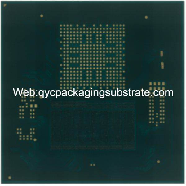
What is ABF Substrate?
Ajimomoto (ABF) Substrate Manufacturer. We have made the FCBGA substrates with the Showa Denko materials: MCL-E-705G, MCL-E-770G, MCL-E-700G, MCL-E-795G. and the Ajimomoto (ABF) series materials.they are:GX92R,
ABF Substrate, Ajinomoto Build-up Film, as a key material specially used to build advanced PCBs, occupies an important position in modern electronic engineering.
Core features of ABF Substrate
ABF Substrate is highly regarded for its unique construction method and excellent performance. As a thin film built on top of electronic devices, it forms complex structures by stacking multiple layers of thin films on a PCB. This structure provides solid support for the electronics and passes signals through the circuit, ensuring excellent signal integrity throughout the system.
The role of ABF Substrate
ABF Substrate plays a vital role in improving the performance and reliability of electronic devices. Primarily, it functions as a foundational building material for Printed Circuit Boards (PCBs), offering versatility in the arrangement and linkage of electronic components. Its exceptional thermal stability and conductivity render it an optimal choice for sophisticated electronic devices that operate within high-temperature environments.
The combination of ABF Substrate and advanced technology
As technology continues to evolve, ABF Substrate has shown strong potential in combination with advanced technologies. Its combination with HDIs (High-Density Interconnects) technology enables PCBs to achieve higher integration and smaller package sizes, thereby promoting the lightweight and compactness of electronic equipment.
ABF Substrate’s future outlook
As a result of relentless innovation in electronic engineering, ABF Substrate stands poised to maintain a pivotal role in the future landscape. Its utilization in next-generation chip packaging technology and the semiconductor industry is slated for further expansion. With escalating demands for performance and reliability in electronic equipment, ABF Substrate will persist in furnishing a dependable foundation for PCB engineering, ensuring its continued significance in advancing technological frontiers.
In PCB design using ABF Substrate, engineers can not only enjoy its excellent performance, but also be able to cope with growing technical challenges. Overall, ABF Substrate, as an important part of electronic equipment manufacturing, has injected new vitality into the continuous development of the industry.
This material, specifically designed to build high-performance PCBs, will undoubtedly drive continuous innovation and progress in the field of electronic engineering in the future.
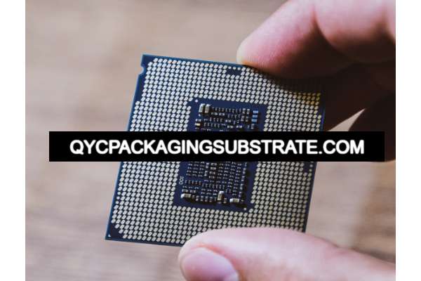
ABF Substrate
What are the functions of ABF Substrate?
ABF Substrate (Ajinomoto Build-up Film substrate), as an important part of modern Printed Circuit Boards (PCBs) engineering, plays a vital function. Get an in-depth look at the capabilities of ABF Substrate as it relates to critical aspects of signal integrity, thermal management, and overall reliability of electronic components.
First, one of the functions of ABF Substrate in PCB is to promote signal integrity.ABF Substrate helps reduce losses during signal transmission and improve signal stability and accuracy through its superior dielectric properties and signal propagation characteristics. This allows electronic devices to transmit and receive information more reliably, thereby improving overall system performance.
Secondly, ABF Substrate plays a significant role in thermal management. In modern electronic devices, high power and high integration are often accompanied by intense heat generation.
The properties of its material make PCBs more resistant to environmental factors such as humidity and temperature changes. This helps extend the life of electronic equipment, reduces failures and damage caused by environmental factors, and improves equipment reliability.
In general, ABF Substrate is not only a substrate material, but also a key element that plays multiple functions in PCB engineering. Through superior signal integrity, thermal management and overall reliability, ABF Substrate promotes performance innovation in electronic devices and supports the continuous development of modern technology.
What types of ABF Substrate are there?
In today’s continuously innovative field of electronic engineering, ABF Substrate (Ajinomoto Build-up Film, amino acid on-film), as a key material, has shown remarkable diversity in its different types of applications. A deep understanding of the different types of ABF Substrates on the market is critical to meeting specific application needs and industry standards. The following will introduce several major ABF Substrate types and their key role in electronic device manufacturing.
Diversity of ABF Substrate types
The diversity of ABF Substrate is reflected in its different types of variants to suit the needs of various electronic applications. These types exist according to changes in performance, thickness, number of layers, etc., and therefore have a wide range of application prospects.
High performance ABF Substrate
In response to the demand for high-performance applications, a range of advanced ABF substrates has surfaced in the market. Distinguished by outstanding thermal conductivity, signal integrity, and robust mechanical stability, these materials stand out as optimal choices for high-performance electronic devices. Within this category, keywords like “high performance,” “thermal conductivity,” and “signal integrity” prominently underscore the distinctive advantages inherent in these substrates.
Ultra-thin ABF Substrate
For some thin and light electronic devices, such as smartphones and tablets, ultra-thin ABF Substrate emerges as the times require. This type of ABF Substrate usually has an extremely thin thickness, providing the possibility for compact design while maintaining good electrical performance. In this context, keywords such as “ultra-thin”, “compact design” and “electrical performance” become prominent features.
Multilayer ABF Substrate
Multi-layer ABF Substrate is designed for applications that require high circuit density. By increasing the number of layers in the vertical direction, this type of ABF Substrate allows electronic devices to integrate more functional units and improves the overall performance of the circuit board. The keywords “multilayer,” “circuit density,” and “functional unit” highlight their importance in increasing system complexity.
Industry Specific ABF Substrate
With the continuous improvement of performance requirements for electronic equipment in various industries, some ABF Substrates specially designed for specific industries have emerged. This includes medical, military, automotive and other fields. These ABF Substrates have unique advantages in meeting special environments and usage conditions. Here, keywords such as “medical”, “military” and “automotive” highlight their industry-specific applicability.
Overall, the diversity of ABF Substrate provides electronic engineers with the flexibility and choice to choose the most appropriate material based on the requirements of a specific application. This also reflects that ABF Substrate, as a key component in PCB engineering, can exert its unique advantages in different fields.
ABF Substrate
How is ABF Substrate different from traditional PCB?
When exploring the differences between ABF Substrate and traditional PCBs, we gain insight into the unique advantages of this advanced material over traditional alternatives. ABF Substrate, or Ajinomoto Build-up Film, as a key element in modern PCB engineering, exhibits many eye-catching features, making it increasingly important in electronic equipment manufacturing.
ABF Substrate is unique in its material composition and performance characteristics. Traditional PCBs usually use glass fiber reinforced epoxy resin as the base material, while ABF Substrate uses Ajinomoto’s unique construction film technology. This film is not only lighter and thinner, but also performs better in high-frequency applications. Its material properties give ABF Substrate significant advantages in improving signal integrity, helping to ensure stable performance of high-speed electronic equipment.
Compared with traditional PCB, ABF Substrate also performs well in thermal management. Its higher thermal conductivity helps effectively disperse the heat generated by electronic components, thereby improving overall system reliability. In application scenarios of high-density integrated circuits and advanced packaging technology, ABF Substrate can better meet the stringent requirements for thermal stability and heat dissipation.
Another obvious difference is in the manufacturing process. The manufacturing of ABF Substrate adopts improved HDI manufacturing technology and semi-additive method, which makes it more flexible in component layout and improves manufacturing efficiency.
These advantages make ABF Substrate occupy an increasingly important position in modern electronic equipment manufacturing, providing engineers with more innovation and design possibilities.
What are the structures and production techniques like?
As a key component of modern PCB engineering, ABF Substrate’s main structure and production technology are crucial to the performance of electronic devices. Below we will delve into the structure and manufacturing process of ABF Substrate, paying special attention to the application of improved HDI manufacturing technology and semi-additive methods.
The main structure of ABF Substrate
The main structure of ABF Substrate includes multi-layer films, of which the ABF film is the key layer to build the substrate. This film has high electrical insulation properties and superior thermal properties, making it ideal for advanced PCBs. In ABF Substrate, the layered structure of the film is carefully designed to ensure optimal signal integrity and electrical performance in dense electronic component layouts.
ABF Substrate’s production technology
High-density interconnect (HDI) manufacturing technology is a key process that enables higher component integration through the use of fine lines and smaller apertures on ABF Substrate. This technology enables more electrical connections in a relatively small space, improving PCB performance. Improved HDI manufacturing technology is widely used in ABF Substrate, further improving the level of device integration on the board through more precise process steps.
Semi-additive method
Semi-additive method is another important production technology, which gradually adds copper layers to the surface of the substrate instead of using the traditional full additive method. This approach reduces scrap production, improves manufacturing efficiency, and helps create more detailed circuit diagrams on ABF Substrate. The application of the semi-additive method makes the manufacturing process more environmentally friendly and can meet the needs of advanced electronic equipment for lightweighting and thinning.
ABF Substrate’s structure and production technology are key elements in modern PCB engineering and directly affect the performance and reliability of electronic equipment. By in-depth understanding of ABF Substrate’s multi-layer thin film structure and the manufacturing technology used, engineers can better respond to changing market demands and lay a solid foundation for innovative electronic products. The application of this advanced material, especially in improved HDI manufacturing technology and semi-additive methods, brings higher reliability and performance levels to PCB engineering.
Chip packaging technology classification?
In today’s evolving electronic technology field, ABF Substrate (Ajinomoto Build-up Film), as an advanced semiconductor material, is closely related to chip packaging technology and provides key support for improving the performance and reliability of electronic equipment.
The integration of ABF Substrate in chip packaging technology is closely related to its unique physical and electrical properties. This material provides the semiconductor industry with a flexible, high-performance solution. Let’s take a deeper look at ABF Substrate’s classification in chip packaging to better understand its role in the semiconductor field.
The relationship between ABF Substrate and chip packaging technology
ABF Substrate plays a key role in chip packaging. Its high degree of insulation and superior thermal conductivity make it an ideal chip packaging material. Through close integration with chip packaging technology, ABF Substrate can meet the high performance and miniaturization needs of modern electronic devices.
One classification of ABF Substrate is based on encapsulation structure. This includes single-sided packaging, double-sided packaging and multi-layer packaging. This classification allows engineers to select the best packaging structure for a specific application.
ABF Substrate, on the other hand, can be classified based on integration technology. This covers traditional Wire Bonding technology and advanced Flip Chip technology. Flip Chip technology improves signal transmission speed and reliability by directly connecting the back of the chip to the Substrate.
ABF Substrate can also be classified according to different packaging materials, such as based on polyimide (PI) and epoxy resin. Each material has unique properties and is suitable for different environments and application scenarios.
ABF SubstrateFAQs
How does ABF Substrate improve PCB performance?
ABF Substrate effectively improves PCB performance through its superior signal integrity and thermal management characteristics. Its highly reliable construction ensures that electronic devices perform well in a variety of application scenarios.
What are the application areas of ABF Substrate?
The ABF substrate finds widespread application in high-performance electronic equipment, including communication devices, computer systems, and embedded systems. Its versatility positions it as an ideal choice across various industries, showcasing its adaptability to diverse technological needs.
Compared with traditional PCB, what are the advantages of ABF Substrate?
Compared with traditional PCB, ABF Substrate has better thermal conductivity, higher integration density and better electrical performance. This makes it popular in modern electronics manufacturing.
How to choose the appropriate ABF Substrate type?
Choosing the appropriate type of ABF Substrate depends on the needs of your specific application. Different types provide flexible options to meet the design requirements of various electronic devices.
How are ABF Substrate and chip packaging technology related to each other?
ABF Substrate plays a key role in chip packaging technology, combining with advanced semiconductor processes to provide reliable support and connections for electronic chips.
What are the technical details worth noting during the manufacturing process of ABF Substrate?
The manufacturing process of ABF Substrate involves improved HDI manufacturing technology and semi-additive methods. These technical details directly affect the quality and performance of the final product.
What is the difference between ABF Substrate and ordinary PCB?
ABF Substrate is different from traditional PCB. Its unique structure and materials give it significant advantages in thermal management, signal integrity and integration density. This difference directly affects the overall performance of the electronic device.