 Professional Flip-Chip Packaging Substrate Supplier

Ajinomoto GL102R8HF package substrate Manufacturer . We use advanced Msap and Sap technology to produce the ABF materials FC BGA package substrates from 2 layer to 22 layers.
With the continuous development of electronic equipment, Ajinomoto GL102R8HF packaging substrate as a key component is gradually coming into people’s field of vision. This cutting-edge technology is changing our understanding of electronic products, bringing more efficient and reliable solutions to all walks of life. The emergence of Ajinomoto GL102R8HF packaging substrate marks the entry of electronic equipment into a new era. Its advanced materials and manufacturing processes will provide strong support for future technological innovation and promote the development of the electronics industry.
What is Ajinomoto GL102R8HF package substrate?
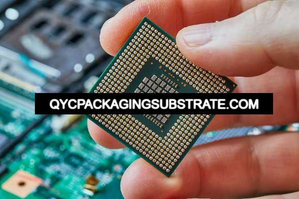
Ajinomoto GL102R8HF Packaging Substrate is a printed circuit board (PCB) that plays a vital role in electronic devices. It not only connects various electronic components, but also provides them with stable and reliable support. As one of the core components of electronic products, Ajinomoto GL102R8HF packaging substrate ensures its reliability and stability in various application scenarios by using high-quality materials and advanced manufacturing processes.
This packaging substrate uses high-quality materials, including high-strength fiberglass as the base material of the substrate, and copper with good conductivity as the conductor layer. In addition, it also applies advanced solder film technology and silk screen printing process to ensure that the electrical and mechanical properties of the circuit board are optimal. These carefully selected materials and processes enable the Ajinomoto GL102R8HF packaging substrate to withstand challenges under various environmental conditions, thereby ensuring the long-term stable operation of electronic products.
Ajinomoto GL102R8HF package substrate Manufacturer
With the Ajinomoto GL102R8HF packaging substrate, electronics manufacturers can achieve higher production efficiency and better product performance. Its compact design and stable performance make it widely used in various application scenarios, including consumer electronics, automotive, aerospace, medical equipment, and communications. Whether it is a small mobile device or a complex industrial control system, Ajinomoto GL102R8HF packaging substrate can provide reliable electrical connection and stable support.
In conclusion, Ajinomoto GL102R8HF packaging substrate is an integral part of modern electronics manufacturing. Its high-quality materials, advanced manufacturing processes and wide range of applications have made it one of the first choices for electronic product manufacturers, bringing them improved reliability, stability and performance.
Ajinomoto GL102R8HF package substrate design Reference Guide.
In the design of modern electronic devices, Ajinomoto GL102R8HF packaging substrate plays a key role. To ensure circuit stability, performance, and reliability, designers need to follow a number of important principles and considerations.
Circuit layout
Circuit layout is one of the core aspects of Ajinomoto GL102R8HF packaging substrate design. Reasonable circuit layout can minimize signal interference and crosstalk, and improve the stability and anti-interference ability of the circuit. Designers need to consider factors such as spacing between electronic components, signal transmission paths, and separation of power and signal lines to ensure good performance of the circuit.
Signal integrity
In the design of Ajinomoto GL102R8HF packaging substrate, ensuring signal integrity is crucial. Signal integrity involves the stability and accuracy of signals during transmission, and is particularly important for the transmission of high-speed signals and high-frequency signals. Designers need to take measures to reduce signal transmission delays, waveform distortion and reflections to ensure reliable signal transmission.
Thermal management
Good thermal management is an aspect that cannot be ignored in the design of Ajinomoto GL102R8HF packaging substrate. Electronic equipment generates a large amount of heat during operation. If the heat cannot be effectively dissipated, it will cause overheating and performance degradation of circuit components. Therefore, it is necessary to rationally arrange heat sinks, heat dissipation holes and thermal conduction paths during the design process to improve heat conduction and dissipation efficiency and ensure the stability and reliability of the circuit.
In summary, the Ajinomoto GL102R8HF Packaging Substrate Design Reference Guide covers important principles and considerations such as circuit layout, signal integrity, and thermal management. Following these guidelines, designers can design electronic devices with high stability and superior performance to meet the needs of different application scenarios.
What material is used in Ajinomoto GL102R8HF package substrate?
Ajinomoto GL102R8HF packaging substrate is a high-performance printed circuit board (PCB) that utilizes a range of carefully selected materials to ensure its excellent stability and reliability under various environmental conditions. The selection of these materials is not only related to the performance of the product, but also directly affects the performance and reliability of electronic equipment.
First of all, Ajinomoto GL102R8HF packaging substrate uses high-strength glass fiber as the base material. Glass fiber has excellent mechanical strength and heat resistance, can remain stable in high temperature and high pressure environments, effectively prevents PCB bending and deformation, and improves the stability of the overall structure.
Secondly, copper is another important material that is used in the conductive layers of PCBs. High-purity copper has excellent electrical conductivity and good weldability, ensuring the stability and reliability of signal transmission.
In terms of solder film, Ajinomoto GL102R8HF packaging substrate uses high-quality solder film material. Solder film is used to cover the soldering area on the PCB surface to protect the solder joints from oxidation and corrosion and ensure the firmness and stability of the soldering connection.
Additionally, silk screen is another critical material used to mark component locations, pin orientations, and other important information on the PCB. Ajinomoto GL102R8HF packaging substrate uses high-resolution silk screen technology to ensure that information is clearly visible and facilitates identification and operation during manufacturing and maintenance processes.
To sum up, the high-performance materials used in Ajinomoto GL102R8HF packaging substrate, such as fiberglass, copper, solder film and silk screen, ensure its excellent stability and reliability under various environmental conditions. The careful selection of these materials and high-quality manufacturing processes make Ajinomoto GL102R8HF packaging substrate an integral part of electronic product manufacturing, providing key support for various application scenarios.
What size are Ajinomoto GL102R8HF package substrate?
Ajinomoto GL102R8HF packaging substrates are available in a variety of size and dimension options for different sizes and types of electronic devices. Whether it’s a tiny portable device or a large industrial device, the Ajinomoto GL102R8HF can meet every need. It has a wide range of sizes, ranging from micro equipment of a few millimeters to large industrial equipment of several meters. There are corresponding models to choose from. This versatility makes Ajinomoto GL102R8HF packaging substrate an ideal choice for a wide range of electronic products.
Not only that, the Ajinomoto GL102R8HF packaging substrate can also be customized according to customers’ specific needs to ensure optimal performance and fit. Whether customers require ultra-thin designs, high-density wiring or specially shaped substrates, Ajinomoto GL102R8HF can provide flexible solutions to meet the needs of various complex applications.
In addition, the flexibility in size of the Ajinomoto GL102R8HF packaging substrate also provides broad room for innovation. Designers can utilize Ajinomoto GL102R8HF in different sizes to achieve various functional and performance requirements, thereby promoting the continuous development and innovation of electronic products. This flexibility not only enables more diverse product designs, but also improves product performance and competitiveness.
In summary, Ajinomoto GL102R8HF packaging substrate not only has wide applicability in terms of size, but also provides customers with customized solutions, providing strong support for the design and innovation of electronic products.
The Manufacturer Process of Ajinomoto GL102R8HF package substrate.
The manufacturing process of Ajinomoto GL102R8HF packaging substrate has been carefully designed and highly processed, ensuring the stability of its quality and performance.
Design
The first step in the manufacturing process is design. At this stage, engineers use advanced CAD software to design the circuit, taking into account the size, hierarchy, and circuit layout of the substrate. The design team is dedicated to ensuring the board’s performance is optimized and cost-effective.
Prototyping
After the design is completed, prototypes are produced for testing and validation. By using advanced prototyping equipment and technology, samples that meet design requirements can be quickly produced. The key to this phase is to ensure that the functionality and performance of the prototype are consistent with the design specifications.
Etching
Etching is one of the key steps in manufacturing the Ajinomoto GL102R8HF packaging substrate. In this process, the metal film covering the surface of the substrate is exposed to a chemical solution to remove unwanted parts. This creates a path between the wires and connecting circuits, ensuring proper functionality of the circuit board.
Drilling
After etching is complete, the next step is drilling. At this stage, precision drilling equipment is used to drill holes into the substrate in order to install electronic components and make circuit connections. The location and size of the drill holes must be precisely controlled to ensure the quality and reliability of the circuit board.
Assembly
The final step is assembly. At this stage, the electronic components are mounted on the Ajinomoto GL102R8HF packaging substrate and soldered. The assembly process requires highly precise operations and strict quality control to ensure that each component is connected correctly and the board is functioning properly.
Through this series of precise manufacturing steps, Ajinomoto GL102R8HF packaging substrate is able to produce high-quality, highly reliable products, providing a solid foundation for performance improvement and stable operation of various electronic devices.
The Application area of Ajinomoto GL102R8HF package substrate.
Ajinomoto GL102R8HF packaging substrate is a key technology in today’s electronics industry. Its wide range of applications covers multiple industries, providing stable and reliable support for various electronic products. The following are the applications of this substrate in different fields:
Consumer Electronics
In the field of consumer electronics, Ajinomoto GL102R8HF packaging substrates are widely used in the manufacture of products such as smartphones, tablets, personal computers and home appliances. Its high performance and reliability ensure the stable operation of the device and provide users with an excellent user experience.
Car
The automotive industry’s demand for electronic technology continues to grow, and Ajinomoto GL102R8HF packaging substrate plays an important role in automotive electronic systems. It is used to manufacture key components such as in-car entertainment systems, vehicle control units, safety systems and navigation systems, improving the intelligence and safety performance of cars.
Aerospace
In the aerospace field, Ajinomoto GL102R8HF packaging substrates are used to manufacture key components such as flight control systems, communication equipment, navigation systems and satellite communication systems. Its high reliability and high temperature resistance enable aerospace equipment to operate stably in harsh environments.
Medical equipment
The medical equipment industry has extremely high requirements for electronic products, and Ajinomoto GL102R8HF packaging substrates are widely used in the manufacture of key equipment such as medical imaging equipment, patient monitoring systems, surgical instruments, and medical diagnostic equipment. Its stability and precise performance ensure accurate diagnosis and treatment results of medical equipment.
Communication
In the field of communications, Ajinomoto GL102R8HF packaging substrates are used to manufacture key equipment such as base station equipment, network routers, optical fiber communication equipment, and mobile communication terminals. Its high-speed data transmission and reliable performance enable communication equipment to meet the growing data transmission needs.
In general, Ajinomoto GL102R8HF packaging substrate has a wide range of applications. Its high performance and reliability make it an indispensable part of the manufacturing of various electronic products, providing strong support for the technological development of modern society.
What are the advantages of Ajinomoto GL102R8HF package substrate?
In modern electronics manufacturing, Ajinomoto GL102R8HF packaging substrate is highly regarded for its excellent performance and multiple advantages. These advantages are detailed below:
Compactness
The Ajinomoto GL102R8HF packaging substrate is exquisitely designed to achieve a compact layout of the circuit, minimize the size of the device, and improve the overall performance and aesthetic appearance of the product. Whether it’s a mobile device or an industrial control system, everyone benefits from its compact design.
Reliability
As a key component of electronic equipment, Ajinomoto GL102R8HF packaging substrates offer excellent reliability and stability. It is made of high-quality materials and undergoes strict quality control and testing to ensure stable operation under various environmental conditions, which greatly improves the reliability and lifespan of the product.
Easy to mass produce
Ajinomoto GL102R8HF packaging substrate adopts advanced manufacturing technology and automated production lines, with high efficiency and high consistency production capabilities. This makes large-scale production possible and meets the market’s demand for high-quality, high-volume supply of electronic products.
Design flexibility
Ajinomoto GL102R8HF packaging substrate has good design flexibility and can meet the design needs of various electronic products. Designers can customize the design according to specific application scenarios and functional requirements to achieve personalized circuit layout and functional combination, thus providing the possibility for product innovation and differentiation.
In summary, Ajinomoto GL102R8HF packaging substrate has become an indispensable part of electronic product manufacturing due to its many advantages such as compactness, reliability, ease of mass production, and flexible design. Whether it is consumer electronics, automobiles, medical equipment, communications and other industries, all can benefit from its excellent performance and reliability, promoting the development and innovation of the entire industry.
FAQ
How much does the Ajinomoto GL102R8HF packaging substrate cost?
The cost of Ajinomoto GL102R8HF packaging substrate depends on several factors, including size, material, design complexity and order volume. Generally speaking, custom Ajinomoto GL102R8HF packaging substrates will be more expensive than standard specs, but they usually offer better performance and adaptability.
What are the environmental impacts of using Ajinomoto GL102R8HF packaging substrate?
The manufacturing process of Ajinomoto GL102R8HF packaging substrate strictly follows environmental standards and is committed to reducing negative impact on the environment. These substrates are often made from recyclable materials and follow sustainability principles to reduce waste generation and energy consumption.
How to recycle Ajinomoto GL102R8HF packaging substrate?
Ajinomoto GL102R8HF packaging substrates can be recycled through specialized e-waste recycling systems. When disposing of discarded Ajinomoto GL102R8HF packaging substrates, ensure that proper disposal procedures are followed to ensure safety for the environment and human health.
How to troubleshoot the Ajinomoto GL102R8HF packaging substrate?
Some malfunctions or issues may occur when using the Ajinomoto GL102R8HF packaging substrate. This situation usually requires systematic troubleshooting steps such as checking circuit connections, testing electronic components, and analyzing circuit board layout. In addition, you can refer to the technical documentation and user manual of the Ajinomoto GL102R8HF packaged substrate for more detailed troubleshooting information.
What design flexibility is available with the Ajinomoto GL102R8HF packaging substrate?
Ajinomoto GL102R8HF packaging substrate offers a high degree of design flexibility and can be customized to meet specific application needs. Users can choose from different materials, layouts and sizes to meet the specific requirements of various electronic products. In addition, Ajinomoto GL102R8HF packaging substrate also supports multi-layer design and high-density integrated circuit layout, providing more space for the implementation of complex circuits.