 Professional Flip-Chip Packaging Substrate Supplier

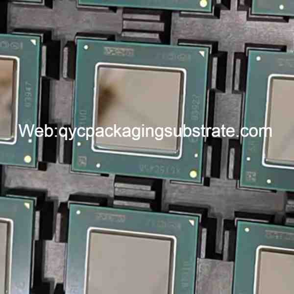
What is BGA Substrate?
BGA substrate manufacturing. and BGA Substrate designed with smallest pitch. to use the advanced Msap and Sap technology. we have produce the microtrace/spacing with 9um/9um.
BGA Substrate (Ball Grid Array Substrate) is a key component widely used in modern electronic equipment, especially in the field of integrated circuit packaging. The core concept of this technology is that it provides reliable support and connection to the chip. Now, let’s dive into the definition and basic concepts of BGA Substrate.
BGA Substrate can be understood as an infrastructure that supports and connects chips. Its name comes from its unique ball grid array arrangement. This arrangement allows BGA Substrate to achieve high-density connections in a relatively small space, providing a more compact and efficient design for electronic devices. Typically, BGA Substrate consists of multiple layers of films that are stacked on top of each other through advanced manufacturing techniques to form a strong and precise structure.
Ball Grid Array Connections: BGA Substrate is unique in that its bottom is covered with tiny solder balls that match the corresponding connection points on the chip. This connection method not only provides a high degree of electrical performance, but also effectively solves a series of problems faced by traditional pad connections.
Multilayer structure: BGA Substrate is usually composed of multiple layers of films, and the stacking of these films forms a complex structure. Each layer performs a specific function, such as providing electrical connections, thermal conductivity or mechanical support.
Advanced manufacturing technology: In the process of manufacturing BGA Substrate, a series of advanced manufacturing technologies are used, such as improved HDI manufacturing technology and semi-additive method. These technologies ensure that the manufactured BGA Substrate has a high degree of precision and reliability.
By deeply understanding the definition and basic concepts of BGA Substrate, we can better grasp its importance in electronic engineering and how it promotes technological innovation and development.
What are the functions of BGA Substrate?
BGA Substrate (Ball Grid Array Substrate) is a key component widely used in modern electronic equipment, especially in the field of integrated circuit packaging. The core concept of this technology is that it provides reliable support and connection to the chip. Now, let’s dive into the definition and basic concepts of BGA Substrate.
BGA Substrate can be understood as an infrastructure that supports and connects chips. Its name comes from its unique ball grid array arrangement. This arrangement allows BGA Substrate to achieve high-density connections in a relatively small space, providing a more compact and efficient design for electronic devices. Typically, BGA Substrate consists of multiple layers of films that are stacked on top of each other through advanced manufacturing techniques to form a strong and precise structure.
Ball Grid Array Connections: BGA Substrate is unique in that its bottom is covered with tiny solder balls that match the corresponding connection points on the chip. This connection method not only provides a high degree of electrical performance, but also effectively solves a series of problems faced by traditional pad connections.
Multilayer structure: BGA Substrate is usually composed of multiple layers of films, and the stacking of these films forms a complex structure. Each layer performs a specific function, such as providing electrical connections, thermal conductivity or mechanical support.
Advanced manufacturing technology: In the process of manufacturing BGA Substrate, a series of advanced manufacturing technologies are used, such as improved HDI manufacturing technology and semi-additive method. These technologies ensure that the manufactured BGA Substrate has a high degree of precision and reliability.
By deeply understanding the definition and basic concepts of BGA Substrate, we can better grasp its importance in electronic engineering and how it promotes technological innovation and development.
BGA Substrate
What are the different types of BGA Substrate?
In the field of electronic engineering, BGA Substrate has attracted much attention due to its various types, each of which exhibits unique advantages and uses in specific application scenarios. Several common BGA Substrate types will be introduced in detail below to better understand their role in modern electronic devices.
There are two primary material-based classifications for BGA (Ball Grid Array) substrates: Organic Substrate and Inorganic Substrate. Organic substrates commonly utilize a base material of glass fiber reinforced epoxy resin. This type of BGA substrate offers notable advantages in terms of lightweight design and cost-effectiveness. This dual classification system allows for a nuanced understanding of BGA substrates, catering to diverse application needs and cost considerations Multi-layer BGA Substrate provides higher electrical connection density by stacking multiple substrates, and is suitable for fields that require higher circuit complexity, such as communication equipment and high-performance computing.
In addition, according to different manufacturing processes, we can also divide BGA Substrate into two categories: traditional process (Traditional Process) and advanced process (Advanced Process). The traditional process uses a relatively simple manufacturing process and is suitable for some scenarios that do not require high performance. The advanced process uses highly precise manufacturing technology to provide higher signal integrity and electrical performance, and is suitable for fields such as high-performance computing and advanced communication systems.
BGA substrates, spanning various types, find extensive applications in electronic engineering. When tasked with selecting the most suitable BGA substrate type for a project, it is essential to carefully weigh project-specific requirements, considering factors such as performance, cost, weight, and environmental compatibility. An insightful comprehension of the distinct characteristics inherent to various BGA substrates empowers engineers to make informed decisions tailored to the actual needs of the project. This ensures that electronic devices not only meet but optimize performance in diverse application scenarios.
What is the relationship between BGA Substrate and IC packaging?
BGA Substrate is closely linked to integrated circuit (IC) packaging, and the synergy between the two plays a key role in modern electronic engineering. As an important component, BGA Substrate provides solid support and connection for the IC. It also has a profound impact on the performance and stability of the chip through its structure and material selection.
First, let’s take a deeper look at the relationship between BGA Substrate and IC packaging. BGA Substrate is an IC-enabled substrate that connects the chip to a printed circuit board (PCB) through its surface mounting technology. Compared with traditional packaging technologies, BGA Substrate provides higher connection density and shorter signal transmission paths, thereby improving the performance and speed of electronic devices.
In terms of chip packaging technology, BGA Substrate involves various types of packaging, including ball grid array (BGA) packaging, leadless packaging (CSP), etc. These package types have different characteristics and are suitable for different application scenarios. BGA packaging achieves higher connection density through its spherical connection points, and is suitable for occasions with higher requirements for high performance and high-density integration. CSP is widely used in some special fields due to its small size and light weight.
BGA Substrate
In addition, chip packaging technology can also be classified according to different processes and materials. Common chip packaging technologies include plastic packaging, ceramic packaging, organic substrate packaging, etc. These classifications reflect the differences in thermal management, electrical performance and cost of different packaging technologies, and also provide electronic engineers with a basis for selecting appropriate packaging technologies in designs.
In practical applications, choosing the appropriate BGA Substrate and chip packaging technology is crucial to the reliability and performance of the overall circuit. By having an in-depth understanding of BGA Substrate and different types of chip packaging technologies, engineers can better optimize designs and ensure that electronic devices achieve optimal performance in all aspects.
Generally speaking, BGA Substrate is closely related to IC packaging, which directly affects the reliability and performance of electronic devices. An in-depth understanding of these relationships will help professionals in the field of PCB engineering better select and apply appropriate technologies and promote continuous innovation in the field of electronic engineering.
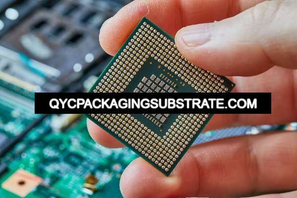
What is the difference between BGA Substrate and PCB?
In the field of electronic engineering, BGA Substrate is closely related to traditional PCB (Printed Circuit Board, printed circuit board), PWB (Printed Wiring Board, printed wiring board), motherboard, Substrate-like PCB (SLP) and HDI Substrate (High-Density Interconnect Substrate). , high-density interconnect substrates), exhibiting unique and eye-catching design and application characteristics.
First of all, the design of BGA Substrate is significantly different from conventional PCB. Traditional PCBs usually have a planar structure, where electronic components are connected to the surface of the board through soldering. BGA Substrate uses ball grid array (BGA) packaging technology to integrate solder balls at the bottom of the component and connect them to the corresponding pads on the substrate. This three-dimensional connection method not only increases the connection density, but also significantly reduces the size of the components, making them more flexible for use in compact spaces.
Secondly, compared to PWB, BGA Substrate pays more attention to electrical performance and signal integrity in design. Due to the three-dimensional layout of solder balls, BGA Substrate can provide shorter signal paths and reduce signal transmission delays, thereby improving system performance. In addition, BGA Substrate makes it easier to implement high-density interconnections, helping to meet the needs for miniaturization and high performance of today’s electronic devices.
In comparison with motherboards, BGA Substrate is usually an important part of the motherboard, responsible for connecting and supporting integrated circuits. The motherboard is larger than BGA Substrate and contains numerous peripheral connections and interfaces, while BGA Substrate focuses more on the interconnection of internal chips and provides a highly integrated solution for the motherboard through its unique design.
Substrate-like PCB (SLP) and HDI Substrate are two derivatives of BGA Substrate. SLP is thinner in design and is suitable for some application scenarios that require higher thickness. HDI Substrate improves the efficiency of signal transmission through high-density interconnection and inter-layer technology and is suitable for applications that require higher signal integrity. high field. Compared with traditional PCB, these two highlight greater flexibility and adaptability.
Overall, BGA Substrate plays a key role in modern electronic engineering through its unique design and application characteristics. Its three-dimensional connection, high-density interconnection and optimized signal transmission performance make it popular in the design of miniaturized, high-performance electronic devices. In today’s pursuit of innovation and excellent performance, the emergence of BGA Substrate undoubtedly provides electronic engineers with a more advanced and efficient solution.
What are the main structures and production technologies of BGA Substrate?
BGA Substrate (Ball Grid Array Substrate) is a key component of electronic equipment, and its design and manufacturing technology directly affect the performance and reliability of the entire system. Let’s dive into the structure of BGA Substrate and some key aspects of its manufacturing technology.
The structure of BGA Substrate is the cornerstone of its performance and functionality. Typically, it consists of multiple layers, each with specific functions and connections. Key elements include electrical connections, power planes, ground planes, signal layers, etc. Through the clever design and layout of these layers, BGA Substrate can implement complex signal transmission, power distribution, thermal management and other functions.
Among them, electrical connections are usually realized through tiny solder balls or pins, forming a unique Ball Grid Array structure. This design provides higher connection density and better electrical performance, making BGA Substrate widely used in modern electronic devices.
The manufacturing technology of BGA Substrate involves a variety of key processes, of which the two main methods are improved HDI (high-density interconnect) manufacturing technology and the semi-additive method.
Improved HDI manufacturing technology
HDI technology improves the wiring density of circuit boards by increasing layers, reducing line width, and narrowing apertures. In the manufacturing of BGA Substrate, improved HDI technology is widely used, making electrical connections more precise and signal transmission more stable. The advantage of this technology is that it can achieve more connections in a limited space and meet the needs of modern electronic devices for miniaturization and high performance.
Semi-additive method
The semi-additive method is an advanced manufacturing technology that only adds the required metal layers during the manufacturing process, avoiding excess materials in the traditional full-additive method. In the manufacturing of BGA Substrate, the semi-additive method not only improves manufacturing efficiency, but also reduces waste generation and is environmentally friendly. This technology has significant advantages in improving manufacturing accuracy and reducing costs.
Through these advanced manufacturing technologies, BGA Substrate can play an important role in miniaturized, high-performance electronic devices. The continuous innovation of its structure and manufacturing technology will continue to promote the development of the field of electronic engineering and inject more possibilities into our scientific and technological life.
BGA SubstrateFAQs
What is BGA Substrate?
Ball Grid Array Substrate (BGA Substrate) stands as a pivotal integrated circuit packaging technology designed primarily for linking chips with motherboards. Its intricate structure comprises multiple layers of conductive and insulating materials, establishing connections with the chip through an array of minute solder balls. BGA Substrate assumes a crucial role in contemporary electronic devices by delivering dependable connections and efficient heat dissipation for high-density, high-performance chips.
How is BGA Substrate different from regular PCB?
Compared with traditional printed circuit boards (PCBs), BGA Substrate focuses more on supporting high-density integrated circuits. It is designed with smaller, more complex chip layouts in mind and uses micro-bending technology to achieve higher solder ball density. This makes BGA Substrate more common in modern electronics, especially in mobile devices and computer systems.
What are the manufacturing technologies of BGA Substrate?
The production of BGA Substrates involves several key steps, including multi-layer printing, conductive layer patterning, and solder ball preparation. Among these, cutting-edge technologies like enhanced HDI (High-Density Interconnect) manufacturing and the semi-additive method play a pivotal role in elevating the performance of BGA Substrates. These technologies go beyond just improving electrical conductivity; they also enhance support for high-frequency signals and bolster heat dissipation capabilities. As a result, they contribute significantly to advancing the overall functionality and efficiency of BGA Substrates.
What is the application scope of BGA Substrate?
BGA Substrate is widely used in various electronic devices, including smartphones, tablets, computers, etc. Its superior performance and reliability make it ideal for handling complex circuit layouts and supporting high-performance chips.
What factors were considered in the design of BGA Substrate?
When designing BGA Substrate, engineers need to consider multiple factors such as electrical performance, heat dissipation effect, and signal integrity. This includes solder ball layout, impedance control of conductive layers, and support for high-frequency signal transmission.
By answering these frequently asked questions, we hope that readers can better understand the nature and application of BGA Substrate and provide strong support for its practical application in the field of electronic engineering.