 Professional Flip-Chip Packaging Substrate Supplier

Ceramic Package Substrate Manufacturer. Ceramic 96 AL2O3 Substrate amd Ceramic ALN Substrate materials. We can use this base materials to make the PCBs. or Ceramic Package Substrates. High quality and fast shipping time.
Primarily, the outstanding rigidity of ceramic packaging substrates is instrumental in maintaining structural stability within high-density circuit layouts—an essential attribute in the contemporary trend towards smaller and lighter electronic products. Furthermore, the high hardness and wear resistance of ceramics enable these substrates to thrive in challenging environments, effectively resisting external shocks and vibrations.
The high thermal conductivity of ceramics positions them as ideal materials for heat transfer, aiding in efficient heat management and dispersion within confined spaces. This, in turn, enhances device performance and reliability.
Beyond their material properties, ceramic packaging substrates shine in their adaptability to diverse design needs in electronic equipment. With the ability to achieve complex geometries and support multi-layer designs, engineers enjoy greater flexibility in circuit layout, meeting the compact design requirements of advanced electronic products.
In summary, ceramic packaging substrates are emerging as an eagerly anticipated innovative solution in the contemporary PCB field, driven by their unique material properties and their pivotal role in electronic device design. With technology’s continuous advancement, the expectation is that ceramic packaging substrates will find even broader applications across various electronic products, ushering in advanced design and manufacturing technologies to the industry.
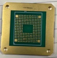
Ceramic Packaging Substrate
What are the types of ceramic packaging substrates?
Mechanical Strength:It possesses ample mechanical strength to withstand various stresses in complex electronic devices.
Applications:Alumina finds ideal use in power amplifiers, RF modules, power modules, and electronic equipment in high-temperature environments, such as aerospace fields.
AlN (Aluminum Nitride) Ceramic Packaging Substrate
AlN ceramic packaging substrates excel in thermal conductivity and chemical stability. Core characteristics encompass:
Superior Thermal Conductivity: Aluminum nitride exhibits excellent thermal conductivity, surpassing other ceramic materials, facilitating rapid heat conduction.
Chemical Stability:AlN resists chemical corrosion, ensuring performance in harsh environments.
Low Dielectric Constant: Its low dielectric constant aids in reducing signal attenuation during signal transmission.
Dimensional Stability:In high-temperature and high-humidity environments, AlN maintains stable dimensions, enhancing equipment reliability.
Applications:AlN is widely employed in high-power electronic modules, LED packaging for heat dissipation, and in microwave and millimeter-wave applications requiring high-frequency performance.
In conclusion, both Alumina and AlN ceramic packaging substrates offer distinct advantages in electronic design. Engineers can judiciously choose the most suitable material based on specific application requirements, ensuring optimal performance and stability in electronic devices.
AlN (aluminum nitride) ceramic packaging substrate
AlN ceramic packaging substrates stand out for their excellent thermal conductivity and chemical stability. The following are the main characteristics of AlN ceramic packaging substrates:
Super thermal conductivity: Aluminum nitride has excellent thermal conductivity, much higher than other ceramic materials, helping to conduct heat quickly.
Chemical Stability: AlN has high resistance to chemical corrosion, allowing it to perform well in harsh environments.
Low dielectric constant: Having a low dielectric constant helps reduce signal attenuation in signal transmission.
Dimensional stability: In high-temperature and high-humidity environments, AlN maintains stable dimensions, helping to improve equipment reliability.
High-power electronic modules: AlN is widely used in high-power electronic modules, such as power inverters.
LED packaging: Due to its excellent thermal conductivity, AlN is often used in LED packaging to help dissipate heat.
Microwave and Millimeter Wave Applications: Excellent in microwave and millimeter wave applications requiring high frequency performance.
Overall, Alumina and AlN ceramic packaging substrates each have their own advantages in electronic design. Engineers can choose the most suitable material according to the requirements of specific applications to ensure the performance and stability of electronic devices.
What are the advantages of ceramic packaging substrates?
In contemporary electronic engineering, ceramic packaging substrates have emerged as a standout choice among various circuit board options, garnering favor from design engineers due to their exceptional performance and a host of advantages. Distinguished by unique characteristics, ceramic packaging substrates surpass traditional circuit boards, particularly in high-tech applications and demanding environments.
In applications featuring high-density integrated circuits and power-intensive devices, this heightened thermal conductivity ensures system stability and reliability.
Furthermore, ceramic packaging substrates exhibit superior mechanical strength compared to traditional organic substrates. The hardness and durability of ceramic materials enable these substrates to maintain structural integrity under mechanical stress and vibrations. This resilience is particularly crucial for devices operating in dynamic and challenging environments, such as automotive electronic systems and military applications.
A remarkable aspect is the outstanding stability of ceramic packaging substrates in high-temperature environments. Ceramic materials retain their structure and performance even under extreme temperature conditions, rendering ceramic packaging substrates indispensable for challenges posed by elevated temperatures. In aerospace, energy, and industrial applications, this property is pivotal for ensuring the reliability of electronic equipment in harsh temperature environments.
Collectively, the high thermal conductivity, excellent mechanical strength, and exceptional stability in high-temperature environments position ceramic packaging substrates as the preferred choice in numerous fields. Their widespread adoption in electronic engineering, especially in areas demanding high performance and reliability, underscores the pivotal role of ceramic packaging substrates in shaping the future of circuit design. Design engineers are actively exploring innovative ways to harness this advanced technology, aiming to propel the performance and stability of electronic devices to unprecedented heights.
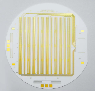
Ceramic Package Substrate
Why choose ceramic packaging substrate?
Within the intricate landscape of electronic equipment design, engineers encounter a multitude of considerations when choosing circuit boards. One increasingly prominent choice in the spotlight is ceramic packaging substrates, and there are compelling reasons why engineers should give them serious consideration.
Secondly, ceramic packaging substrates exhibit outstanding mechanical strength. In environments prone to extreme conditions, such as aerospace or automotive electronic systems, where equipment may encounter severe vibration and shock, ceramic substrates excel. Their robust mechanical strength enables them to effectively withstand external challenges, guaranteeing the stability and reliability of the circuit board.
Furthermore, ceramic packaging substrates shine in high-temperature environments. Certain applications, like aerospace or high-performance computing equipment, necessitate operation under extreme temperature conditions. Ceramic substrates can endure higher operating temperatures, preserving the performance of electronic components and rendering them suitable for demanding applications.
The design flexibility of ceramic packaging substrates is another notable feature. Their adaptable design can accommodate diverse and complex circuit layouts while optimizing space utilization. This characteristic is particularly crucial in the design of modern portable devices, contributing to the compactness and lightweight nature of products like smartphones and tablets.
In summary, the compelling reasons for choosing ceramic packaging substrates lie in their superior performance in thermal conductivity, mechanical strength, high-temperature stability, and design flexibility. In the realm of high-performance and specialized applications, ceramic packaging substrates emerge as advanced solutions that engineers should genuinely contemplate.
What is the manufacturing process of ceramic packaging substrates?
The production of ceramic packaging substrates is a highly intricate and precise undertaking, exerting direct influence on the performance and reliability of the end product. Let’s delve into this intricate manufacturing process, concentrating on pivotal steps at both the motherboard and substrate levels and the substantial influence these steps wield over the final performance.
Overview of the Manufacturing Steps
Material Preparation:The process initiates with the meticulous preparation of necessary materials, typically alumina (Alumina) or aluminum nitride (AlN), chosen for their commendable thermal conductivity and mechanical strength.
Board Pre-treatment:Prior to entering the manufacturing process, boards undergo rigorous pre-treatment, involving cleaning, impurity removal, and surface treatment to ensure material purity and workability.
Circuit Design and Creation:At the motherboard level, circuit graphics are meticulously designed and crafted. This involves utilizing CAD software to draft the circuit layout, accounting for signal routing, component placement, and overall circuit architecture.
Printing:Employing layer-by-layer printing technology, circuit graphics are incrementally added to the ceramic substrate. Precision in the printing process is paramount to meet design specifications.
Welding and Metallization:At the substrate level, circuits on different layers are interconnected through welding, and metallization is executed to enhance conductivity—crucial for ensuring circuit smoothness.
Blind Hole Drilling:For intricate circuit board designs, blind hole drilling becomes essential, requiring sophisticated equipment to guarantee accuracy in hole diameter and depth.
Sintering and Heat Treatment:Ceramic packaging substrates undergo a sintering process to densify and fortify their structure. Subsequent heat treatment ensures stability and optimal thermal conductivity.
Impact of Manufacturing Processes
Thermal Conductivity:Delicate sintering and heat treatment profoundly impact the thermal conductivity of ceramic packaging substrates, enhancing the material’s ability to efficiently transfer and disperse heat.
Mechanical Strength:Material pretreatment and welding, among other steps, significantly determine the mechanical strength of ceramic packaging substrates. Meticulous workmanship ensures the board is resistant to cracking or deformation during use.
Signal Transmission Quality:The precision of printing and welding processes directly influences circuit quality. Ensuring accuracy and control at each step enhances the stability and quality of signal transmission.
Stability:Crucial steps like sintering and heat treatment play a pivotal role in the stability of ceramic packaging substrates. They guarantee material performance stability under extreme temperature conditions, rendering them suitable for diverse application environments.
By comprehending the intricacies of the ceramic packaging substrate manufacturing process, we gain a nuanced understanding of the significance of each step and the profound impact these processes have on the final product’s performance. This insight equips engineers with a comprehensive perspective when designing and selecting ceramic packaging substrates.
In what fields are ceramic packaging substrates widely used?
Recognized as a cutting-edge circuit board material, the ceramic packaging substrate has proven its adaptability across a wide array of applications, asserting itself as an essential component spanning from smartphones to medical equipment. Its importance lies in its distinctive attributes, enabling outstanding performance and demonstrating versatility in a variety of settings.
Primarily, ceramic packaging substrates assume a pivotal role in the realm of smartphones. With the perpetual evolution of smartphones demanding higher performance and compact designs, ceramic substrates prove ideal due to their remarkable thermal conductivity and mechanical strength. Ensuring stability and reliability, these substrates enable electronic components to function seamlessly in the elevated temperature environment within mobile phones, while their flexibility aligns with the continual innovation in mobile phone design.
Ceramic packaging substrates play a pivotal role in the realm of medical devices, offering crucial support to meet the stringent requirements for accuracy and reliability in medical equipment. Their stability and high thermal conductivity make ceramic substrates the preferred choice, extending their applications from implantable medical devices to portable monitoring equipment, contributing significantly to the manufacturing of various medical devices.
Beyond the medical field, ceramic packaging substrates find extensive utility in aerospace, military equipment, and industrial control systems. Their exceptional performance in demanding conditions such as high temperatures, humidity, and intensity underscores their indispensability in these sectors. The reliability and durability of ceramic substrates ensure the stable operation of electronic equipment even in extreme environments.
In summary, the diverse applications across various industries highlight the versatility and adaptability of ceramic packaging substrates. Their successful integration into high-tech domains like smartphones and medical equipment expands the possibilities for electronic engineers. As technology continues to advance, ceramic packaging substrates are expected to maintain their key role, driving innovation and development across a spectrum of industries.
How to obtain ceramic packaging substrates?
Obtaining ceramic packaging substrates is a critical decision involving successful product design and manufacturing. Readers can obtain ceramic packaging substrates through many ways, among which suppliers and manufacturers are one of the practical ways to obtain such circuit boards.
Acquiring ceramic packaging substrates can be achieved through two main channels: collaboration with specialized suppliers and direct engagement with manufacturers. Professional suppliers, focusing on electronic components and circuit boards, offer a primary avenue for customers to explore a wide range of ceramic packaging substrate options. Building strong partnerships with these suppliers affords customers access to a diverse selection, customization opportunities, and competitive pricing.
When selecting a supplier, customers should consider critical factors such as reputation, industry experience, and a dedication to product quality. Opting for a reputable supplier ensures that the ceramic packaging substrates meet the expected standards of reliability and performance.
The second strategy involves a direct collaboration with manufacturers, providing customers with more personalized solutions to meet specific design requirements. Manufacturers typically possess advanced production equipment and process technology, enabling the delivery of tailor-made ceramic packaging substrates of high quality aligned with customer specifications.
Engaging directly with manufacturers allows customers to actively participate in the design and manufacturing process, ensuring the final product adheres to precise technical and performance standards. This close partnership facilitates streamlined communication, cost reduction, and heightened production efficiency.
Ultimately, readers have the flexibility to choose the approach that aligns best with their needs and preferences when procuring ceramic packaging substrates. Opting for specialist suppliers offers a wide selection and competitive prices, whereas direct collaboration with manufacturers delivers highly customized solutions. For certain companies, obtaining ceramic packaging substrates through direct supply chain relationships may be the most convenient choice. Regardless of the selected method, it remains crucial to ensure the professionalism and reliability of the partner to guarantee that the final product meets expected standards of quality and performance.
What is the quotation for ceramic packaging substrates?
Securing a precise quote for ceramic packaging substrates is a crucial undertaking, involving a nuanced consideration of various factors. Here are key considerations when selecting a supplier for ceramic packaging substrates and navigating the quoting process.
Secondly, the number of layers and the complexity of ceramic packaging substrates impact their price. Increased layers and intricate designs may necessitate additional manufacturing steps, elevating production costs. During the design phase, engineers must judiciously assess these aspects to meet project requirements while managing costs effectively.
Moreover, the order quantity plays a role in determining the price of ceramic packaging substrates. Generally, high-volume production can lower the cost per unit, while low-volume production may incur higher manufacturing costs. Engineers should make reasonable estimates of production quantities early in the design stage, facilitating negotiations with manufacturers for favorable quotes.
Finally, additional costs in the manufacturing process, such as design modifications, special process requirements, and delivery time, can impact the final quotation. Clear communication with manufacturers regarding these needs enhances mutual understanding of the project’s complexity and cost structure.
In conclusion, obtaining an accurate quote for ceramic packaging substrates necessitates meticulous consideration of multiple factors, spanning material selection to manufacturing processes. Collaborating with an experienced manufacturer and addressing these factors early in the design process ensures a successful project implementation that aligns with both project requirements and budget constraints.
What are the common problems with ceramic packaging substrates?
Are ceramic packaging substrates susceptible to thermal shock?
Ceramic packaging substrates exhibit commendable thermal conductivity, although their vulnerability to thermal shock in the face of drastic temperature fluctuations necessitates a careful assessment contingent upon the particular material and design. Superior ceramic packaging substrates, known for their high quality, typically demonstrate resilience against thermal shock.
Are ceramic packaging substrates susceptible to signal distortion in high-frequency applications?
Ceramic packaging substrates typically feature a reduced dielectric constant, resulting in generally lower signal distortion. However, in high-frequency applications, the nuances of design and meticulous material selection remain crucial and require comprehensive consideration.
Are the thermal expansion coefficients matched between the ceramic packaging substrate and the metal package?
A mismatch in thermal expansion coefficients can cause stress between the ceramic package substrate and the metal package, affecting performance. During the design phase it is necessary to ensure that material selection takes into account matching coefficients of thermal expansion.
Are ceramic packaging substrates susceptible to mechanical vibration?
Ceramic packaging substrates typically exhibit robust mechanical strength. However, in environments characterized by high-frequency vibrations, the design considerations must carefully assess the potential impact of mechanical oscillations on their reliability.
Is the process of manufacturing ceramic packaging substrates complicated?
The production procedure for ceramic packaging substrates is intricately detailed and demands a high level of precision. When selecting a manufacturer, it is essential to take into account their expertise and experience to ensure a meticulous and skillful manufacturing process.
Is the cost of ceramic packaging substrates higher than traditional substrates?
The pricing of ceramic packaging substrates typically tends to be higher, with the cost hinging primarily on the selected ceramic material and the intricacies of the manufacturing process. When devising a design, it becomes imperative to carefully assess the advantages and disadvantages in accordance with specific requirements and budget constraints.