 Professional Flip-Chip Packaging Substrate Supplier

What is Ceramic Packaging Substrate?
Ceramic packaging substrate manufacturer. the Package Substrate will be made with Ceramic ALUMINUM AL2O3, Ceramic 96 AL2O3, ALN Ceramic base materials. or other types Ceramic materials.
The Ceramic Packaging Substrate stands at the vanguard of innovation within the PCB realm, assuming a pivotal role in facilitating the connection and support of electronic components. This fundamental component not only redefines the benchmarks for circuit board design but also fosters seamless electrical connections within electronic devices. In doing so, it becomes a catalyst for technological advancements, ushering in improved performance and setting the stage for further breakthroughs in the field.
Its unique design and material selection allow it to demonstrate superior capabilities in connecting electronic components. As an innovative basic component, Ceramic Packaging Substrate has a multi-layered design designed to provide excellent electrical performance and thermal management.
Ceramic Packaging Substrate is designed to enable efficient connections between electronic components. By using ceramic materials, it provides superior electrical and thermal conductivity, providing a solid foundation for device reliability and performance. This advanced connection method allows electronic components to be more tightly integrated and achieve efficient transmission of electrical signals.
In the realm of PCB innovation, the advent of Ceramic Packaging Substrate marks a revolutionary leap forward. In stark contrast to traditional substrates, the Ceramic Packaging Substrate boasts a lighter and more compact profile, enhancing the flexibility of electronic device designs. Leveraging advanced manufacturing technology and meticulous material selection, it excels in accommodating high-density circuit layouts, providing robust support for the rapid evolution of modern electronic equipment.
The introduction of Ceramic Packaging Substrate not only reshapes the internal architecture of electronic devices but also achieves seamless electrical connections. Its design not only prioritizes the optimization of electrical performance but also comprehensively addresses the requirements of thermal management. This implies that during high loads and frequencies, the equipment can efficiently dissipate heat, ensuring steadfast stability and reliability.
As technology marches forward, the Ceramic Packaging Substrate is poised to continue playing a pivotal role in electronic engineering. Its exceptional performance and adaptable design render it ideal for the next generation of electronic devices. From cutting-edge connection technologies to efficient thermal management, Ceramic Packaging Substrate is set to steer the developmental trajectory of future electronic devices.
In summary, the introduction of Ceramic Packaging Substrate instigates a revolution in PCB engineering. By redefining the approach to connecting and supporting electronic components, it unfurls new possibilities for innovation and the development of electronic devices. The ongoing progression of this technology will undoubtedly propel the electronic engineering field forward, injecting renewed vigor into our technological future.
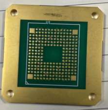
Ceramic Packaging Substrate
What types of Ceramic Packaging Substrate are there?
The rapid strides in PCB (Printed Circuit Board) engineering have significantly heightened the significance of Ceramic Packaging Substrates in propelling innovation in electronic design and manufacturing. Among these substrates, those founded on aluminum oxide and aluminum nitride have emerged prominently, showcasing distinctive characteristics that cater to specific design requirements and contribute to the continuous advancement of electronic engineering.
Taking center stage, Alumina-based Ceramic Packaging Substrates have found extensive application in high-power and high-frequency scenarios. Acknowledged for their outstanding insulation properties and high thermal conductivity, alumina substrates excel in demanding, high-temperature environments, ensuring steadfast performance under challenging conditions. The robust mechanical strength of aluminum oxide further amplifies its suitability for deployment in extreme environments.
In contrast, Ceramic Packaging Substrates based on aluminum nitride are highly sought after for their outstanding thermal conductivity and low dielectric loss properties. Specifically designed to handle high power density and high-frequency signals, aluminum nitride substrates provide reliable support for advanced electronic devices. The superior thermal conductivity of aluminum nitride positions it as an excellent performer in thermal management, serving as a dependable channel for heat dissipation from electronic components. This versatility makes these substrates crucial elements in the ever-evolving landscape of electronic engineering.
The unique characteristics of each Ceramic Packaging Substrate type enable engineers to make precise selections based on specific design requirements. For instance, in scenarios involving high temperatures or extreme conditions, an aluminum oxide-based substrate may be preferable. On the other hand, applications with heightened demands for thermal conductivity and low dielectric losses may find aluminum nitride-based substrates more suitable. This multifaceted selectivity empowers engineers to choose the most fitting substrate type, thereby advancing electronic engineering.
The proliferation of diverse Ceramic Packaging Substrate types has breathed new life into electronic engineering. By providing options tailored to various application scenarios, engineers gain the flexibility to design and manufacture advanced electronic devices with greater adaptability. This not only caters to current electronic engineering needs but also establishes a robust foundation for future technological innovations.
In summary, Ceramic Packaging Substrates unveil their immense potential in electronic engineering through their diverse types. This diversity not only expands the choices available to engineers but also leads to groundbreaking improvements in the performance and reliability of electronic equipment. As technology evolves, Ceramic Packaging Substrates are poised to maintain a vital role in the electronics field, propelling the industry forward.
What are the advantages of Ceramic Packaging Substrate?
In contemporary PCB engineering, Ceramic Packaging Substrate has emerged as a focal point, showcasing remarkable electrical performance and cutting-edge thermal management capabilities. This innovation has significantly influenced electronic design and manufacturing processes. The numerous advantages of Ceramic Packaging Substrate span across enhanced electrical performance, advanced thermal management, increased efficiency, heightened reliability, and the facilitation of electronic device miniaturization. This versatile material is revolutionizing the landscape of electronic components, providing a comprehensive solution for diverse engineering challenges.
This substrate performs well when transmitting signals, reducing signal transmission losses, thus ensuring the high-performance operation of electronic equipment. Its excellent dielectric constant and low loss characteristics allow signals to propagate more efficiently, providing an ideal solution for high-frequency applications.
Advanced thermal management capabilities
The ceramic material used in Ceramic Packaging Substrates boasts exceptional thermal conductivity properties, rendering it an optimal solution for efficient thermal management. In contemporary electronic devices, maintaining precise temperature control is imperative to guarantee the secure and stable operation of components. By adeptly conducting and dispersing heat, Ceramic Packaging Substrates play a pivotal role in diminishing component temperatures, thereby enhancing overall reliability and performance in electronic equipment.
Improve the efficiency of electronic equipment
By providing superior electrical performance and thermal management, Ceramic Packaging Substrate directly impacts the overall efficiency of electronic devices. Lower signal transmission loss ensures accurate signal transmission and reduces energy loss in the system. At the same time, excellent thermal management ensures that the equipment maintains efficient working status during long-term operation, thus improving the overall performance of the equipment.
Improve electronic equipment reliability
Ceramic Packaging Substrate improves the reliability of electronic devices through the stability and high durability of ceramic materials. This substrate maintains its performance in the face of changing work environments and working conditions, reducing the risk of component failure caused by environmental changes. This provides longer life and greater stability for critical application scenarios.
Promote the miniaturization of electronic equipment
The superior performance of Ceramic Packaging Substrate allows the design of more compact and miniaturized electronic devices. Its highly integrated features allow electronic components to be laid out in a smaller space, providing an ideal solution for modern portable devices and miniaturization applications.
Overall, Ceramic Packaging Substrate’s advantages in electrical performance and thermal management directly bring significant improvements to the efficiency, reliability and miniaturization of electronic devices. The application of this innovative substrate is leading a new trend in electronic engineering, paving the way for future high-performance devices.
Why choose Ceramic Packaging Substrate?
In today’s rapid development of PCB engineering, Ceramic Packaging Substrate, as a trend-leading technology, has injected new vitality into electronic design and manufacturing. So, why choose Ceramic Packaging Substrate instead of traditional PCB among many circuit boards? This article will compare their advantages in depth, demonstrate the excellence of Ceramic Packaging Substrate from the perspective of performance, compact design and adaptability to emerging technologies, and illustrate its advantages in certain scenarios through examples.
Excellent performance
Ceramic Packaging Substrate distinguishes itself through its exceptional electrical properties. In contrast to conventional PCBs, ceramic substrates exhibit enhanced stability in high-frequency and high-temperature settings, significantly elevating the overall performance of electronic devices. Specifically, in radio frequency (RF) applications, Ceramic Packaging Substrate excels in signal conduction, minimizing signal loss and thereby enhancing the reliability of communications.
Compact design
Ceramic Packaging Substrate is more compact in design, effectively reducing the size of electronic equipment. In comparison, traditional PCBs may require larger space to achieve similar functions. This miniaturized design makes Ceramic Packaging Substrate ideal for mobile devices, drones and other space-constrained applications, bringing greater flexibility to product design.
Adapt to emerging technologies
With the emergence of emerging technologies, Ceramic Packaging Substrate can more easily adapt to advanced processes and materials. Its high temperature stability and adaptability to new materials make it an ideal platform for integrating advanced technologies. For example, when it comes to 5G communications, artificial intelligence processors and other fields, Ceramic Packaging Substrate can better cope with the challenges of high temperature and high performance, providing a broad space for innovation.
Overall, Ceramic Packaging Substrate has proven its advantages over traditional PCBs through excellence in performance, compact design and adaptability to emerging technologies, as well as successful applications in multiple industries. Taking these advantages into consideration when selecting a circuit board will help push the forefront of innovation in electronics design and manufacturing.
How is Ceramic Packaging Substrate made?
Ceramic Packaging Substrate is a key component of PCB engineering, and its complex manufacturing process is the driving force for the continuous evolution of the electronic design and manufacturing fields. Production from motherboard to substrate involves key steps, the application of advanced materials and the role of technology in shaping these substrates.
In the manufacturing of Ceramic Packaging Substrate, the production of the motherboard is a crucial step. This process encompasses the clever application of subtractive and additive manufacturing techniques, providing a solid foundation for Ceramic Packaging Substrate’s structure.
Subtractive manufacturing techniques carve out the desired structure by removing unwanted material. The accuracy of this step is critical to the final performance of the motherboard, so advanced CNC machines and precision engraving processes are indispensable.
Additive manufacturing technology builds the motherboard structure by stacking materials layer by layer. 3D printing technology played a key role at this stage, providing Ceramic Packaging Substrate’s complex structures with a high degree of customizability.
The emphasis is on the utilization of cutting-edge materials and technologies, specifically advanced conductive ceramics, to ensure the motherboard maintains optimal conductivity and stability while accommodating electronic components. A crucial aspect of the Ceramic Packaging Substrate manufacturing process is the production of substrates, involving ceramic techniques to establish high-density interconnects that offer reliable support and connections for electronic components.
The employment of ceramic materials, such as aluminum oxide and aluminum nitride, is pivotal in achieving superior substrate manufacturing. Aluminum oxide serves as an insulating layer for substrates, owing to its exceptional insulating properties, while aluminum nitride contributes to thermal management due to its high thermal conductivity.
By incorporating these materials and employing meticulous manufacturing processes, Ceramic Packaging Substrate achieves higher density interconnections, excelling in miniaturized designs and meeting high-performance requirements. This careful selection of materials and attention to critical steps result in a highly customizable product with excellent electrical performance and stable thermal management, making it an ideal choice for modern electronic device designs.
Throughout the manufacturing process, the continuous integration of advanced technologies has injected new vitality into Ceramic Packaging Substrate, prompting it to make revolutionary progress in the field of PCB engineering. This evolving manufacturing process provides smaller, higher-performance solutions for electronic devices and drives technology forward.
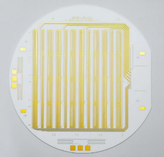
Ceramic PCB
What are the application areas of Ceramic Packaging Substrate?
Ceramic Packaging Substrate stands as a pioneering force in contemporary PCB engineering, serving as a fundamental element in electronic design and manufacturing. Its remarkable performance and extensive applications across diverse industries underscore its significance. This article delves into the varied sectors where Ceramic Packaging Substrate excels, showcasing its versatility and robustness, from aerospace to telecommunications.
In the aerospace sector, electronic equipment must meet rigorous standards, demanding components that exhibit exceptional resistance to high temperatures and vibrations. Ceramic Packaging Substrate has proven to be highly successful in applications such as navigation systems, communication equipment, and satellite technology. Its superior thermal management and structural stability play a crucial role in providing reliable support for various aerospace projects.
In the medical industry, where stability and reliability are paramount for electronic equipment, Ceramic Packaging Substrate finds widespread use. It is prominently featured in medical devices, including patient monitoring equipment, medical imaging tools, and diagnostic instruments. The excellent performance of Ceramic Packaging Substrate ensures the precision and dependability of these critical medical technologies.
Auto industry
In automotive electronic systems, Ceramic Packaging Substrate supports advanced automotive technologies through its superior heat resistance and stability. From engine control modules to advanced driver assistance systems, Ceramic Packaging Substrate delivers higher performance and reliability.
Automated industry
Overall, Ceramic Packaging Substrate plays an irreplaceable role in many fields such as aerospace, communications, medical, automotive and industrial automation with its excellent performance and diverse characteristics. Its wide application not only promotes technological progress in various industries, but also provides electronic engineers with more innovative possibilities. Through in-depth application in these fields, Ceramic Packaging Substrate is leading the development direction of future electronic design.
Where to find Ceramic Packaging Substrate?
When embarking on the journey of electronic engineering, the choice of a dependable and top-notch Ceramic Packaging Substrate holds paramount importance for the success of your project. To assist in making a well-informed decision, consider the following guidelines for pinpointing leading manufacturers and distributors.
The duration of a manufacturer’s tenure often serves as a testament to their prowess in handling intricate projects and overcoming technical challenges. This track record enhances the likelihood of receiving high-quality products and accessing professional guidance when navigating complex requirements.
Understanding a supplier’s technical capabilities and innovativeness is critical to ensuring your project takes full advantage of Ceramic Packaging Substrate. Technologically advanced suppliers may offer more advanced, customizable solutions to meet your specific design requirements.
Consider establishing long-term relationships with suppliers. Such a partnership may provide you with a better understanding of its product lines, services and support. By building a strong partnership, you can more easily resolve potential issues and ensure support throughout the life of the project.
If your company is a manufacturer or distributor of Ceramic Packaging Substrate, you may prioritize in-house supply. In-house provision often provides closer collaboration, greater transparency, and faster response times. This helps ensure you get the best solution for your project needs.
Research case studies and customer feedback from Ceramic Packaging Substrate vendors. This can give you real-world experience on how they tackle similar projects and challenges. Understanding the success stories and challenges of other customers can help you better evaluate whether a vendor is a good fit for your needs.
By carefully selecting your Ceramic Packaging Substrate supplier, you will be able to ensure a successful project implementation. Remember to do adequate research before choosing to ensure you are working with industry-leading manufacturers and distributors to provide the best support and solutions for your project.
How is the quote for Ceramic Packaging Substrate determined?
As a key component of modern electronic design, Ceramic Packaging Substrate’s quotation not only reflects its excellent performance, but is also affected by many factors. In this article, we will delve into the various factors that influence Ceramic Packaging Substrate quotations, aiming to provide readers with the knowledge to gain insight and overcome cost challenges.
The initial factor influencing the quotation of Ceramic Packaging Substrates is the substrate type. Various ceramic substrates, including those derived from aluminum oxide or aluminum nitride, exhibit distinct physical properties and entail varying manufacturing complexities. These factors directly influence production costs, necessitating a meticulous consideration of performance requirements and project budget during the substrate type selection process.
Secondly, considering the continuous evolution of electronic equipment, complexity has become one of the key factors affecting Ceramic Packaging Substrate’s quotation. High-density interconnects, miniaturized designs, and advanced thermal management technologies will increase the complexity of the manufacturing process. Therefore, highly customized designs and advanced manufacturing processes will have a direct impact on the quotation.
Production volume is also a key factor in determining Ceramic Packaging Substrate’s quotation. Scale effects play an important role in the manufacturing process, and mass production can reduce the manufacturing cost of a single substrate. Conversely, low-volume production may result in increased unit costs. Therefore, when developing a project plan, it is crucial to understand and balance the relationship between throughput and cost.
Understanding these factors is like having a beacon for the reader through the quotation puzzle. Understanding how substrate type, complexity and throughput relate to each other can help inform informed decisions and ensure projects move forward within budget.
To address cost challenges, manufacturers often offer diverse substrate options to meet different project needs. From affordable standard models to highly customized special designs, readers can choose the most suitable Ceramic Packaging Substrate based on project requirements.
Overall, understanding these key factors behind the Ceramic Packaging Substrate offer is key to successful electronic design. While pursuing excellence in performance and innovation, sensitivity to cost considerations will enable projects to remain viable. By fully understanding these factors, readers will be able to move to the forefront of electronics design with greater confidence.
Frequently Asked Questions
How are Ceramic Packaging Substrates manufactured?
The manufacturing process involves both motherboard and substrate production. Techniques include subtractive and additive manufacturing for motherboards, while substrates utilize ceramic materials like Alumina and Aluminum Nitride, employing advanced technologies for precision.
Are Ceramic Packaging Substrates compatible with advanced technologies?
Yes, Ceramic Packaging Substrates are highly compatible with advanced technologies. Their superior thermal management and electrical performance make them well-suited for applications involving cutting-edge electronic components.
Where can one source reliable Ceramic Packaging Substrates?
Reputable manufacturers and distributors in the electronics industry offer reliable Ceramic Packaging Substrates. Well-established companies with a track record of quality products are advisable sources for procuring these advanced substrates.
How are Ceramic Packaging Substrate quotes determined?
Ceramic Packaging Substrate quotes depend on factors such as substrate type, complexity of design, and production volumes. Understanding these factors is crucial for project planning and budgeting.
Are Ceramic Packaging Substrates customizable for specific project requirements?
Yes, Ceramic Packaging Substrates are highly customizable to meet specific project requirements. Engineers can work with manufacturers to tailor substrates based on their unique design and functionality needs.