 Professional Flip-Chip Packaging Substrate Supplier

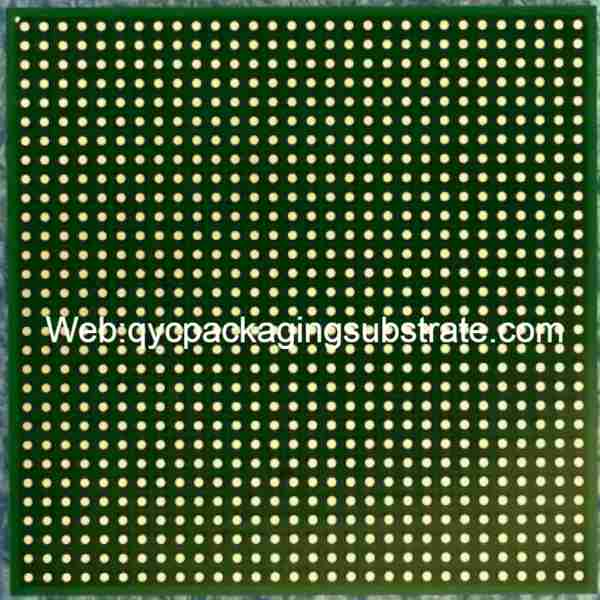
Chip Package Substrate Manufacturer. we can produce the best samllest bump pitch with 100um, the best smallest trace are 9um,and the smallest gap are 9um. most of the design are 15um to 30um trace and spacing.
In the contemporary digital era, electronic devices have seamlessly woven themselves into every facet of our lives. From smartphones to household appliances, from automobiles to medical equipment, electronic technology has evolved into an indispensable facet of modern existence. At the heart of this transformation lies the rapid advancement of chip technology, which has propelled electronic devices to become increasingly compact, potent, and smarter.
Chips, functioning as the core of electronic devices, serve as the driving force behind information processing and transmission. However, these diminutive electronic wonders necessitate proper protection and encapsulation to ensure their performance, reliability, and durability. This is precisely where chip packaging emerges as a critical factor. Chip packaging involves the incorporation of a chip within a protective casing, serving the dual purpose of shielding the chip from physical harm and facilitating efficient thermal management to safeguard the seamless operation of electronic devices.
In this article, we embark on an in-depth exploration of the fundamental component of chip packaging, namely, the chip packaging substrate. These substrates assume a pivotal role in the electronics industry, not only furnishing steadfast support but also playing a pivotal part in circuit connections and performance optimization. We delve into diverse substrate types, their manufacturing processes, and their multifaceted roles across various application domains. Additionally, we cast a forward-looking gaze into the future of chip packaging substrates, shedding light on how innovation and sustainable practices are steering the course of the electronics industry. Join us as we closely examine the chip packaging substrate, unveiling its central role in the realm of modern electronics.
Chip package substrate
What is a chip packaging substrate?
Chip packaging substrates, commonly referred to as packaging substrates, stand as one of the most critical components in electronic equipment, serving as a fundamental material that underpins the functionality of integrated circuit chips and carries out a multitude of crucial functions. Firstly, they furnish robust mechanical support, ensuring secure chip connection to the circuit board. Secondly, these substrates facilitate electrical connections between circuits, enabling the transmission of signals and power.
Beyond establishing electrical connections, they contribute to device miniaturization, making them lighter and more portable. Furthermore, these substrates play a pivotal role in the realm of communication, supporting diverse communication devices ranging from mobile phones to satellite communication systems, facilitating rapid data transfer and wireless communication. In addition, they assume critical importance in the automotive sector, being employed in vehicle control systems, entertainment systems, and safety functions, thereby elevating the performance and convenience of automobiles.
In essence, packaging substrates form the cornerstone of the modern electronics industry. They enhance our lives by enhancing convenience and connectivity, and they drive ongoing innovation and technological development. Hence, acquiring a profound understanding of the various types of packaging substrates and their multifaceted roles across industries is paramount for comprehending the operating principles and future developmental trends of electronic devices.
Types of chip packaging substrates
Various types of substrate materials are commonly employed in electronic packaging, each characterized by distinct properties and applicability:
Silicon Substrate: Silicon substrates are frequently used in chip packaging, offering high electrical conductivity and mechanical stability. They are prevalent in the fabrication of high-density integrated circuits (ICs) due to silicon’s excellent electrical properties, especially for transmitting high-frequency signals. Moreover, silicon substrates demonstrate exceptional mechanical stability, making them ideal for compact packages such as microprocessors.
Organic Substrates: Organic substrates typically employ resin-based materials like FR-4 and are widely utilized in printed circuit board (PCB) manufacturing. These substrates are characterized by their lightweight nature, cost-effectiveness, and excellent electrical insulation properties. They find suitability in various electronic devices, spanning from consumer products to industrial applications.
Ceramic Substrates: Ceramic substrates, often crafted from alumina ceramics, exhibit outstanding thermal conductivity and electrical insulation. They are extensively employed in high-power electronic equipment, including high-frequency RF modules and power amplifiers. Ceramic substrates excel at dissipating heat, rendering them valuable in equipment requiring extended, high-load operation.
Metal Substrates: Metal substrates make use of materials like copper or aluminum and are essential for applications demanding superior thermal conductivity. They are frequently found in LED packages and high-power semiconductor devices. Metal substrates effectively dissipate heat, ensuring a stable operating temperature for electronic components.
Highlight the characteristics and suitability of each substrate
Ceramic Substrates: Ceramic substrates come into their own in high-power RF and microwave electronics, ensuring unwavering stability and performance, essential in these applications.
Metal Substrates: Metal substrates are indispensable in scenarios necessitating exceptional heat dissipation, such as in LEDs and power semiconductors, where temperature control is critical for optimal operation.
The crux of the matter lies in selecting the right substrate type tailored to your specific project’s needs, ensuring optimal performance and unwavering reliability in your application.
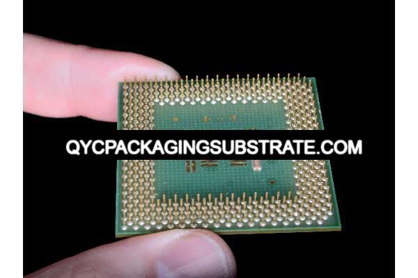
Chip package substrate
Manufacturing process
The production of chip packaging substrates is an intricate and meticulous process critical to the chip’s connection and protection. The following provides an outline of the chip packaging substrate manufacturing procedure, encompassing crucial stages and the significance of material selection.
Substrate Preparation: The initial phase in the manufacturing sequence entails preparing the substrate. The selection of the substrate hinges upon the application’s specific requirements and may encompass materials like silicon, organic compounds, ceramics, or metals. A special surface treatment is imperative to guarantee strong adhesion and solderability, ensuring the substrate’s suitability for its intended role.
Circuit Design and Printing: Circuit design is the next step where the designer creates the circuit layout on the substrate. After this, printing techniques are used to deposit a conductive material, usually copper, on the substrate. These conductive lines form the basis of electrical circuits.
Material stacking: A key step in the manufacturing process is stacking different layers of materials together to create a multi-layered structure. This involves adding insulating material between conductive layers to ensure the circuit does not short out.
Forming and Drilling: Next, the substrate is formed into the desired shape and drilled in specific locations for subsequent component mounting and connection.
Surface Treatment: A critical step in the manufacturing process is surface treatment of the substrate to enhance its corrosion resistance and solderability. This usually involves adding a special protective coating to the substrate surface.
Component mounting: Once the substrate is prepared, various chips and other electronic components can be precisely mounted onto it. This requires highly sophisticated equipment and technology.
Soldering and Packaging: The next step in connecting the component to the substrate is soldering, usually using solder paste or wire. Once connections are made, the substrate may need to be encapsulated to provide physical protection and thermal management.
Critical Steps and Importance of Material Selection
Within the manufacturing process, several pivotal stages and meticulous material selections hold sway. The careful choice of substrate materials, conductive materials, and insulating materials wields a profound influence on both circuit performance and reliability. Material attributes such as thermal conductivity, adhesion, and resistance to corrosion must align seamlessly with the unique requisites of the application at hand.
Furthermore, each juncture in the manufacturing process demands precise control and vigilant monitoring to guarantee the ultimate packaging substrate for the chip attains the zenith of quality. Any missteps or defects have the potential to precipitate performance discrepancies or outright malfunctions.
In short, the manufacturing of chip packaging substrates is a precise and complex project, which provides the basis for the reliability and performance of modern electronic devices. The importance of critical steps and material selection cannot be underestimated as they directly impact the quality and performance of the final product.
Circuit connections and performance
Circuit connections and performance play a key role in the design and manufacturing of chip packaging substrates. This section will provide an in-depth discussion of the impact of substrate on circuit performance and how to achieve reliable circuit connections, emphasizing criticality and diversity.
Effect of substrate on circuit performance
The choice of chip packaging substrate plays a pivotal role in shaping circuit performance. Diverse substrate types, which encompass silicon, organic, ceramic, and metal substrates, each bring forth unique electrical and thermal properties. Silicon substrates, celebrated for their exceptional thermal conductivity, emerge as ideal candidates for applications in high-temperature settings, such as high-performance computing. Organic substrates, renowned for their lightweight construction and cost-effectiveness, carve out a niche in mobile devices. Ceramic substrates, on the other hand, shine in their ability to offer excellent insulation properties, making them a prime choice for high-frequency electronic equipment. Meanwhile, metal substrates are highly regarded for their capacity to deliver outstanding EMI (electromagnetic interference) suppression performance, rendering them a fitting option for wireless communication equipment.
Furthermore, the thickness and layering of the substrate also hold sway over circuit performance. Thin substrates typically exhibit lower inductance and capacitance, rendering them suitable for high-frequency applications, while thicker substrates may be better suited for power electronics applications.
How to achieve reliable circuit connections
Achieving reliable circuit connections is critical for chip packaging. Connection methods such as soldering, bonding and conductive adhesives need to meet high performance and reliability requirements. Welding is a common connection method, but attention must be paid to temperature control and solder joint strength. Bonding is an important technology in microelectronics packaging, which connects the chip to the substrate through metal wires or solder balls. Conductive adhesive is a flexible option especially suitable for complex circuit designs.
In addition to connection methods, proper design can also improve the reliability of circuit connections. Proper wiring and heat dissipation design can reduce thermal stress between circuit components and extend circuit life. In addition, the use of high-quality connection materials and manufacturing processes also has a positive impact on reliability.
In summary, circuit connections and performance are key factors in chip packaging substrate design, and they directly affect the performance and reliability of electronic devices. Proper selection of substrate type, consideration of layering and connection methods, and use of high-quality materials and workmanship all contribute to superior circuit performance and reliability. These factors jointly promote continuous innovation and progress in the electronic field.
The future of chip packaging substrates
In the field of electronics, technology continues to evolve, and chip packaging substrates must follow this trend to meet growing needs and challenges. The following is an outlook for the future of chip packaging substrates:
Explore future technology trends
Smaller size and higher density: Future chip packaging substrates will pursue smaller size and higher component density.
Multi-layer stacking technology is poised to become increasingly prevalent to cater to the demands of intricate circuits. This innovative approach involves the stacking of multiple substrates to augment circuit density and enhance overall performance.
Faster data transmission speed: With the continuous development of communication technology, future chip packaging substrates will support faster data transmission speeds to meet the requirements of high-speed data processing.
Integrated packaging and thermal solutions: Future substrates will be more integrated while providing more effective thermal solutions to cope with the heat generated by high-performance chips.
Emphasis on the importance of innovation and sustainability
Innovation and sustainability are key to the future development of chip packaging substrates. To meet growing demand, manufacturers will continue to drive technological innovation to develop more efficient and sustainable substrate materials and manufacturing processes. This includes:
Environmentally Conscious Materials: Employ biodegradable and eco-friendly materials to curtail environmental harm and enhance sustainability.
Enhanced Energy Efficiency: Enhance manufacturing procedures to curtail energy usage and diminish the carbon footprint.
Reusability: Design substrates for recycling and reuse, reducing waste.
Supply chain sustainability: Establish a sustainable supply chain to ensure sustainable procurement and production of raw materials.
In summary, future chip packaging substrates will continue to evolve to meet the changing needs of the electronics industry. Technological innovation and sustainable practices will drive progress in this area, providing higher performance, more sustainable solutions for our modern electronic devices.