 Professional Flip-Chip Packaging Substrate Supplier

Extra small pitch PCB manufacturing. We use advanced Msap and Sap technology to produce the High multilayer interconnection PCB and package substrates from 4 to 22 layers.
In today’s electronic equipment, Extra Small Pitch PCB (ultra-fine pitch printed circuit board) plays an increasingly important role. These PCBs not only enable higher integration, but also provide better performance for small devices. As modern electronic products have increasingly higher requirements for volume and performance, the demand for Extra Small Pitch PCB is also growing. This article aims to provide readers with a comprehensive guide to help them better understand and apply this key technology by delving into the design, manufacturing and cost aspects of Extra Small Pitch PCB.
What is Extra Small Pitch PCB?
Extra Small Pitch PCB (ultra-fine pitch printed circuit board) is a printed circuit board characterized by very small spacing between electronic components, usually less than 0.5mm. The purpose of this kind of PCB design and manufacturing is to achieve higher integration and more complex circuit functions in a limited space. Compared with traditional PCB, Extra Small Pitch PCB has higher density and superior performance, and is suitable for various micro electronic devices.
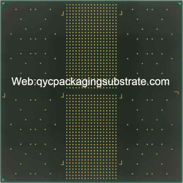
Extra small pitch PCB manufacturing
In micro devices, Extra Small Pitch PCB plays a vital role. First, they provide compact circuit connection solutions for miniature devices, allowing devices to achieve more functions in a limited space. Secondly, Extra Small Pitch PCB can greatly reduce the size and weight of the device, making the micro device more lightweight and portable. In addition, because Extra Small Pitch PCB has higher integration and better performance, it can improve the overall performance and stability of micro devices and meet the needs of modern consumer electronics for compact size and powerful functions.
In short, Extra Small Pitch PCB is a PCB type designed to meet the needs of micro devices for compact, high-performance circuit solutions. It is widely used in micro-devices and provides important support for the development and popularization of modern technology products.
How to design Extra Small Pitch PCB?
Designing Extra Small Pitch PCB is a complex and precise work that requires an in-depth understanding of its basic principles and rigorous steps. The process of designing such a PCB will be introduced in detail below:
Determine the needs: Before designing the Extra Small Pitch PCB, you first need to clarify the needs and specifications of the project. This includes determining the circuit’s functionality, performance specifications, size constraints, and operating environment requirements. This step is crucial for subsequent design work because it will directly affect PCB layout and component selection.
PCB layout design: After determining the project requirements, the next step is to carry out PCB layout design. This process includes sizing the PCB, laying out circuit components and routing. For Extra Small Pitch PCB, the space is more limited, so the layout needs to be carefully designed to ensure that the distance between circuit components is small enough to meet the requirements of high-density integration.
Routing design: Routing is an important step in connecting circuit components, especially critical for Extra Small Pitch PCB. In the wiring design, factors such as signal transmission stability, electromagnetic compatibility, and minimum spacing requirements need to be considered. Multi-layer PCB designs are usually used to increase wiring flexibility and reduce signal interference.
Signal integrity analysis: For Extra Small Pitch PCB, signal integrity is particularly important. Signal integrity analysis needs to be performed during the design process, including clock distribution, signal transmission line matching, impedance control, etc. This helps ensure the stability and reliability of signal transmission.
Thermal management design: Since Extra Small Pitch PCBs are often used in high-performance devices, thermal management design is crucial. This includes rational layout of heat dissipation components, optimizing circuit layout to improve air circulation, selecting appropriate heat dissipation materials, etc. Through effective thermal management design, the stability and reliability of the PCB during long-term operation can be ensured.
Simulation and verification: After the design is completed, simulation and verification are required to ensure the accuracy and reliability of the design. Conduct signal transmission simulation, thermal analysis, etc. through circuit simulation software to verify the feasibility of the design solution. In addition, prototype verification is also required, including PCB sample production and functional testing, to ensure that the design meets the expected requirements.
In general, designing Extra Small Pitch PCB requires comprehensive consideration of multiple factors such as circuit functionality, size constraints, signal integrity, and thermal management. Only on the basis of an in-depth understanding of the basic principles can a high-performance, high-reliability Extra Small Pitch PCB be designed.
What is the manufacturing process of Extra Small Pitch PCB?
The manufacturing process of Extra Small Pitch PCB usually includes the following main steps: design preparation, material selection, pattern drawing, printing, etching, drilling, electroplating, assembly and testing.
First, the designer prepares design documents based on the customer’s needs and specifications, determining the size, number of layers, wiring and component layout of the PCB, etc. Then, an appropriate substrate material is selected, typically fiberglass-reinforced epoxy (FR-4).
Next, the design file is transferred to a printing house, where photolithography is used to imprint the design pattern on the surface of the substrate. Then, through chemical etching, the unnecessary parts of the copper foil are removed from the substrate, leaving the desired circuit pattern.
Then drill the required connection holes on the circuit board. After drilling is completed, electroplating is performed to increase the conductivity and corrosion resistance of the connection hole by plating a layer of metal inside the hole.
Finally, the PCB is assembled and tested. The assembly process includes soldering components to the PCB surface, installing connectors and other accessories, etc. After the assembly is completed, electrical and functional tests are performed to ensure that the PCB meets the design requirements and works properly.
Compared with the traditional PCB manufacturing process, the Extra Small Pitch PCB manufacturing process has some significant differences in some key steps.
First, the design phase requires higher precision and technical requirements. Since Extra Small Pitch PCB has a higher integration level and smaller spacing, designers need to layout and route more carefully to ensure the stability and reliability of the circuit.
Secondly, during the printing and etching processes, more sophisticated equipment and processes are required. Due to the particularity of Extra Small Pitch PCB, higher precision in printing and etching is required to ensure the clarity and accuracy of circuit graphics.
Additionally, higher precision and technology are required during drilling and plating processes. Extra Small Pitch PCB usually has smaller connection holes and thinner wires, so more delicate drilling and plating processes are required to ensure the quality and stability of the connection holes.
In general, compared with the traditional PCB manufacturing process, the manufacturing process of Extra Small Pitch PCB is more complex and sophisticated, requiring higher technical levels and equipment requirements, but it can also provide higher performance and reliability for electronic devices.
How much does Extra Small Pitch PCB cost?
The cost of Extra Small Pitch PCB is an important factor to consider during the manufacturing process, which directly affects the budget and economics of the overall project. It is crucial to understand the factors that affect the cost of Extra Small Pitch PCB, and we will detail these factors below:
PCB design complexity: Design complexity is one of the main factors affecting the cost of Extra Small Pitch PCB. Complex designs require more engineer time and resources to complete, so costs increase accordingly. For example, if the PCB needs to support multiple layers, high-density wiring, special materials, or special process requirements, the manufacturing cost will usually be higher.
PCB size and number of layers: The size and number of layers of the PCB will also directly affect its cost. Generally speaking, larger size or multi-layer PCBs require more materials and processing steps, so the cost will be relatively higher. In contrast, smaller size or single-layer PCBs cost less.
Material selection: The cost of PCB also depends on the materials selected. Prices for different materials vary greatly, and different applications may require specific materials to meet performance and reliability requirements. For example, flexible PCBs generally cost more to manufacture than rigid PCBs, and high-frequency applications may require special high-frequency materials, which are often more expensive.
Production volume: Production volume is also an important factor affecting the cost of Extra Small Pitch PCB. Generally speaking, high-volume production reduces unit costs because the fixed costs of a production line can be spread over more products. In contrast, unit costs for low-volume production are usually higher.
Manufacturing process and technology: The manufacturing process and technology level of PCB will also directly affect its cost. High-precision processes and advanced technologies often increase manufacturing costs, but also provide PCBs with higher quality and performance.
Finished product testing and quality control: Finally, finished product testing and quality control are also important factors affecting the cost of Extra Small Pitch PCB. These processes require additional equipment and labor costs but ensure the quality and reliability of the final product.
To sum up, the factors that affect the cost of Extra Small Pitch PCB include design complexity, size and number of layers, material selection, production volume, manufacturing process and technology, as well as finished product testing and quality control. These factors need to be considered when developing a budget and selecting a manufacturer to ensure a successful project.
What material is Extra Small Pitch PCB made of?
Material selection for Extra Small Pitch PCB (ultra-fine pitch printed circuit board) is critical to its performance and stability. When designing and manufacturing this type of PCB, engineers typically consider a variety of factors, including electrical characteristics, mechanical strength, heat resistance, and cost. Let’s take a look at the commonly used Extra Small Pitch PCB materials.
FR-4 is one of the most commonly used PCB substrate materials. It is composed of fiberglass and epoxy resin and has excellent mechanical strength and heat resistance. FR-4 substrate is suitable for most general applications, providing stable performance and reliability.
High TG FR-4 is an improved FR-4 material with a higher glass transition temperature (TG value) and therefore better heat resistance. This material is suitable for applications that need to operate in high-temperature environments, such as automotive electronics, industrial control and other fields.
Polyimide is a high-temperature, high-performance material with excellent electrical properties and high temperature resistance. It is commonly used in applications that require operation in extreme temperature conditions, such as electronic equipment in the aerospace and defense sectors.
PTFE is a low dielectric constant and low loss material with excellent high frequency characteristics. Therefore, it is often used in Extra Small Pitch PCB designs that require high-frequency transmission and microwave applications.
Metal substrate is a special PCB material whose substrate is made of metal material (such as aluminum or copper) and provides good heat dissipation performance. It is suitable for applications that need to handle high power and heat, such as LED lighting and power amplifiers.
Choosing the right material is crucial for designing and manufacturing Extra Small Pitch PCB. Engineers need to comprehensively consider the electrical properties, mechanical properties, cost and other factors of the material based on the requirements of the specific application to ensure that the PCB meets the expected performance and reliability requirements in actual applications.
Who makes Extra Small Pitch PCB?
The manufacturing of Extra Small Pitch PCB is a highly precise process that requires professional equipment and technology. In this area, manufacturers play a vital role. Let’s take a closer look at who makes Extra Small Pitch PCB.
In the process of manufacturing Extra Small Pitch PCB, choosing the right manufacturer is crucial. Our company is committed to becoming one of the industry’s leading Extra Small Pitch PCB manufacturers. We have advanced production equipment and a professional team to provide high-quality, high-reliability Extra Small Pitch PCB products.
First of all, we have advanced production lines and equipment to meet various Extra Small Pitch PCB manufacturing needs. We use advanced printing technology and precision processing technology to ensure that every PCB has consistent quality and performance.
Secondly, we have an experienced and skilled team. Our engineers and technicians have undergone rigorous training and professional certification, and can provide a full range of technical support and solutions. Whether it is PCB design, process optimization or quality control, we are able to provide our customers with the best service and support.
In addition, we focus on communication and cooperation with customers. We adhere to the principle of “customer first, quality first” and wholeheartedly provide customers with customized solutions. We know that our customers’ needs are diverse, so we are committed to establishing long-term and stable cooperative relationships with our customers to develop and grow together.
Key Features of Excellent Customer Service
A quality Extra Small Pitch PCB manufacturer should have the following key characteristics in providing customer service:
Prompt response: A quality manufacturer should be able to respond quickly and promptly to customer needs and questions. Whether it is inquiry, technical support or after-sales service, manufacturers should assist customers with high efficiency and agility.
Expertise: Manufacturers should have extensive industry experience and expertise and be able to provide customers with accurate, reliable advice and solutions. They should understand all aspects and technical requirements of Extra Small Pitch PCB manufacturing and be able to provide customized services according to the specific needs of customers.
Customized solutions: A quality manufacturer should be able to provide customized solutions as per the specific needs and requirements of the customers. They should be able to flexibly adjust production processes and technical parameters to meet customers’ individual needs and provide customers with the best products and services.
Good communication: Manufacturers should maintain good communication with customers to ensure that both parties agree on project progress, technical details, and quality requirements. They should be able to understand the needs and opinions of customers and provide timely communication and feedback to ensure that the project proceeds smoothly and meets customer expectations.
After-sales support: A quality manufacturer should be able to provide customers with comprehensive after-sales support and services. Whether it is product quality issues, technical difficulties, or other needs, manufacturers should be able to respond promptly and provide solutions to ensure customer satisfaction and trust.
FAQS
What are the main advantages of Extra Small Pitch PCBs?
Extra Small Pitch PCBs offer several advantages, including higher integration density, improved signal integrity, and reduced electromagnetic interference (EMI). Their compact size makes them ideal for miniaturized electronic devices where space is limited.
What factors affect the cost of manufacturing Extra Small Pitch PCBs?
The cost of manufacturing Extra Small Pitch PCBs depends on various factors such as the complexity of the design, the type of materials used, the number of layers, and the production volume. More intricate designs and specialized materials may lead to higher manufacturing costs.
How can I ensure the reliability of Extra Small Pitch PCBs?
To ensure the reliability of Extra Small Pitch PCBs, it is essential to adhere to industry standards for design, manufacturing, and testing. Employing high-quality materials, rigorous quality control processes, and thorough testing procedures can help enhance the reliability and performance of these PCBs.
What are the common challenges in manufacturing Extra Small Pitch PCBs?
Common challenges in manufacturing Extra Small Pitch PCBs include maintaining precise tolerances during fabrication, preventing signal distortion and crosstalk, and ensuring adequate heat dissipation in compact designs. Addressing these challenges requires careful design consideration and close collaboration between designers and manufacturers.