 Professional Flip-Chip Packaging Substrate Supplier

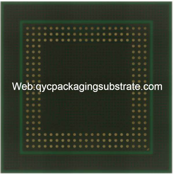
What is FC-BGA Substrate?
FC-BGA Substrate Manufacturer. We use the advanced Sap and Msap technology to produce the small pitch BGA substrate. The smallest spacing and trace are 9um/9um. the smallest via holes size are 50um.
FCBGA Substrate, or Fine-Pitch Ball Grid Array Substrate, is an advanced and critical packaging substrate technology. In the field of electronic device manufacturing, FCBGA Substrate plays a vital role, with its design and functionality aimed at achieving high performance, high-density electrical connections, effective thermal conduction, and mechanical support.
This packaging substrate technology has a wide range of applications, covering many key components of modern electronic devices. FCBGA Substrate is usually used for the packaging of integrated circuits (ICs), providing a reliable connection platform for chips. Its applications are not limited to specific types of equipment, but cover high-performance computing, communication equipment, and various consumer electronics products. Its application in these areas enables equipment to be more compact, efficient and maintain excellent performance in various environments.
In the design of FCBGA Substrate, important keywords include “Fine-Pitch” and “Ball Grid Array”. Fine-Pitch means that it has a smaller pin pitch, making connections closer and helping to achieve highly dense circuit designs. Ball Grid Array emphasizes its spherical arrangement of pins. This design helps improve the reliability and stability of the connection.
Its importance in electronic equipment is not only reflected in providing electrical connections, but also in thermal conduction and mechanical support. Through effective thermal conduction design, FCBGA Substrate can help electronic devices better dissipate the heat generated and ensure that the chip maintains a stable temperature during high-load operation. At the same time, its solid mechanical support ensures the stability of the chip during device operation and movement, reducing the risk of possible damage caused by mechanical vibration and shock.
Overall, FCBGA Substrate is not only a packaging substrate technology, but also a key driving force for improving the performance of modern electronic equipment. Its high degree of integration, efficient connectivity and reliability provide a solid foundation for innovation in the electronics industry and will continue to play an irreplaceable role in future technological development.
What are the functions of FC-BGA Substrate?
FCBGA Substrate, the Fine-Pitch Ball Grid Array packaging substrate, is a key electronic packaging technology and plays an indispensable role in modern electronic equipment. Its main functions cover electrical connection, thermal conduction and mechanical support, providing a stable and reliable foundation for electronic devices.
First, FCBGA Substrate demonstrates its excellent performance in terms of electrical connections. Through the finely arranged Ball Grid Array, it achieves highly dense connections, effectively reduces resistance and inductance, and ensures the stability of signal transmission. This design makes the electrical connection between the chip and the PCB more reliable, effectively supporting the overall performance of the device.
Secondly, FCBGA Substrate plays an important role in heat conduction. Electronic devices generate a large amount of heat when running, and FCBGA Substrate effectively conducts heat to the external environment of the device through its superior heat dissipation design, ensuring that the chip operates within a suitable temperature range. This helps prevent performance degradation or damage to the chip due to overheating, providing a solid foundation for device reliability and stability.
Finally, FCBGA Substrate also plays a key role in mechanical support. Its structural design aims to provide effective support for the chip and prevent adverse effects on the chip from vibration, shock or external stress. This mechanical support not only helps extend the life of the chip, but also provides a solid foundation for the device in various application scenarios, especially in mobile devices and industrial fields.
Taken together, FCBGA Substrate provides advanced and reliable solutions for the manufacturing of modern electronic equipment with its excellent electrical connection, thermal conductivity and mechanical support functions. Its application not only improves the performance and stability of equipment, but also promotes the development of the entire electronics industry. In the ever-changing scientific and technological progress, FCBGA Substrate will continue to play a key role, leading the wave of innovation in the electronic field.
What types of FC-BGA Substrate are there?
As a key innovation in printed circuit board (PCB) technology, FCBGA Substrate covers a variety of types, each of which plays a unique role in specific scenarios. The choice of these types depends on factors such as needs, application scenarios, and performance requirements.
Types of FCBGA Substrate
Single-layer FCBGA Substrate: Single-layer FCBGA Substrate is a relatively basic type and is commonly used in cost-sensitive application scenarios.
This type is usually used in areas with high requirements on space efficiency and signal integrity, such as high-performance computing equipment and communication base stations.
High-density interconnect (HDI) FCBGA Substrate: HDI FCBGA Substrate focuses on high-density interconnection and achieves a more compact design through fine lines and small-pitch stacking levels. This type is widely used in mobile devices such as smartphones and tablets where board space is severely restricted.
Different types of applications in scenarios
Single-layer FCBGA Substrate performs well in cost-sensitive scenarios, such as household appliances and some low-power embedded systems.
HDI FCBGA Substrate HDI FCBGA Substrate plays a key role in mobile devices due to its high-density interconnect characteristics. The huge space compression requirements of smartphones, tablets and other devices are met by HDI FCBGA Substrate.
In different application scenarios, choosing the appropriate type of FCBGA Substrate can best meet the performance, space and cost requirements of the device. This diversity makes FCBGA Substrate an indispensable technological innovation in the field of electronic engineering.
What is the relationship between FCBGA Substrate and IC packaging?
In the field of IC (integrated circuit) packaging, FCBGA Substrate (Fine-Pitch Ball Grid Array Substrate) plays a key role and is closely related to chip packaging technology. This packaging substrate not only provides electrical connections, thermal conductivity and mechanical support functions, but also provides a reliable foundation for different types of chip packaging technologies.
First, let us understand how FCBGA Substrate is related to chip packaging technology in IC packaging. FCBGA Substrate is mainly used to connect chips and printed circuit boards (PCB), and realize chip packaging through tiny ball grid arrays (BGA). This design not only makes the connection more compact, but also improves the reliability of signal transmission. FCBGA Substrate provides a stable and efficient packaging environment for the chip through its precise structure, allowing the chip to perform optimally in various applications.
In the practice of IC packaging, there are multiple chip packaging technologies, which differ in terms of connection, heat dissipation, space utilization, etc. These technologies are divided into different categories based on their characteristics, some of which mainly include:
BGA (Ball Grid Array) packaging technology: This is a common packaging technology in which the pins of the chip are connected to the packaging substrate in the form of a spherical grid. FCBGA Substrate plays an important role in BGA packaging, achieving highly integrated chip connections through its fine ball grid design.
CSP (Chip Scale Package) packaging technology: CSP is a small packaging technology. The size of the package is close to the actual size of the chip, reducing the overall package size. FCBGA Substrate provides reliable electrical connections in the CSP package, allowing the chip to be highly integrated in a smaller space.
QFN (Quad Flat No-Leads) packaging technology: This packaging technology adopts a leadless design and is connected by soldering metal pads on the bottom of the chip. The superior thermal conductivity properties of FCBGA Substrate have significant advantages in QFN packaging, helping to improve the heat dissipation effect of the chip.
WLP (Wafer-Level Package) packaging technology: This is a technology for packaging at the wafer level, which can achieve a high degree of automated production. FCBGA Substrate supports the high integration and efficiency of WLP packaging technology through its manufacturing process.
Through these different chip packaging technologies, FCBGA Substrate meets the needs of different application scenarios and provides high-performance, high-reliability packaging solutions for electronic devices. In the rapid development of the modern electronics industry, FCBGA Substrate, as a key component of IC packaging, provides advanced technical support for various application fields.
How is FC-BGA Substrate different from traditional PCB?
Compared with traditional Printed Wiring Boards (PWBs) and PCBs, FCBGA Substrate (Fine-Pitch Ball Grid Array Substrate) shows significant differences in structure and function. This advanced packaging substrate technology plays an indispensable role in the manufacturing of electronic devices, and its uniqueness is highlighted in the following aspects.
First of all, in terms of structure, FCBGA Substrate adopts a highly dense and complex multi-layer design. Compared with traditional single- or double-layer PCBs, FCBGA Substrate achieves a higher level of integration through a multi-layer structure. This design not only allows for the placement of more signal and power layers, but also provides more flexible routing options, providing more headroom for the performance of electronic devices.
Secondly, FCBGA Substrate far exceeds the scope of traditional PCBs in terms of functionality. As a key component of IC packaging, FCBGA Substrate not only provides electrical connections and thermal conductivity functions, but also plays an important role in mechanical support, packaging and protection of chips. This is in clear contrast to traditional PCBs, which mainly focus on providing circuit connections.
Compared with traditional PCBs, FCBGA Substrate also shows obvious differences in Motherboard, Substrate-like PCB (SLP) and HDI Substrate. The motherboard plays a key role in connecting various components, while FCBGA Substrate focuses more on the packaging and connection of chips. In contrast, although high-density packaging technologies such as Substrate-like PCB (SLP) and HDI Substrate also pursue high integration, FCBGA Substrate is more widely used in IC packaging because it focuses on meeting the high performance of chip packaging. need.
In terms of manufacturing process, FCBGA Substrate uses advanced HDI manufacturing technology and semi-processing methods. Compared with the manufacturing process of traditional PCBs, this advanced technology ensures the high performance and high reliability of FCBGA Substrate. Improved HDI manufacturing technology allows smaller-sized components to be arranged at higher density levels, while the semi-processing method brings higher precision and controllability to the manufacturing process.
Overall, FCBGA Substrate is in sharp contrast to traditional PCBs with its complex multi-layer structure, comprehensive functional design and advanced manufacturing technology. As today’s electronic equipment increasingly pursues high performance and miniaturization, FCBGA Substrate, as an advanced packaging substrate technology, plays a key role in achieving this goal.
What are the structure and production technology of FCBGA Substrate?
The structural design and manufacturing technology of FCBGA Substrate (Fine-Pitch Ball Grid Array Substrate) play a key role in the field of modern electronic packaging. Let’s take a deep dive into the structure and production technology of FCBGA Substrate and learn about the innovations and improvements.
Structural design of FCBGA Substrate
The structural design of FCBGA Substrate is to meet the requirements of high density and high performance, ensuring reliable electrical connection and heat dissipation in a limited space. Its typical structure includes a multi-layer design, each layer carrying a specific function. Key elements include:
Substrate: The substrate of FCBGA Substrate usually uses high-performance insulating materials, such as advanced glass fiber reinforced resin. This substrate not only has good insulation properties, but can also meet high temperature and high frequency requirements.
Interconnect Layers: The interconnect layer is the key to connecting the chip and external devices. HDI manufacturing technology (High-Density Interconnect) allows more interconnections to be implemented in a limited space, thereby increasing connection density and performance.
Pin/Ball Array: This is an important part of connecting FCBGA Substrate and other components. Ball array designs typically use a fine layout, called Fine-Pitch, to ensure highly reliable connections.
Manufacturing technology of FCBGA Substrate
The manufacturing technology of FCBGA Substrate involves many key aspects, among which HDI manufacturing technology and semi-processing method are the highlights.
Application of HDI manufacturing technology: HDI manufacturing technology plays a vital role in FCBGA Substrate. It achieves higher connection density by using tiny lines and holes in the interconnect layer.
Through these advanced manufacturing technologies, FCBGA Substrate can achieve higher integration, more reliable connections and better heat dissipation performance.
Overall, FCBGA Substrate is an advanced packaging substrate technology, and its continuous innovation in structure and manufacturing technology has promoted the development of the electronics industry in the direction of smaller and higher performance. The application of this technology not only improves the performance of electronic devices, but also provides a solid foundation for future innovation.
FCBGA Substrate的FAQs
In what fields is FCBGA Substrate widely used?
FCBGA Substrate, as an advanced packaging substrate technology, is widely used in many fields. It mainly involves high-performance computing, communication equipment, consumer electronics and other fields. Its key features, such as highly dense and reliable connectivity, make it useful in scenarios where high performance and compact packaging are required.
What is the difference between FCBGA Substrate and other packaging substrates?
Compared with traditional Printed Wiring Boards (PWBs) and PCBs, FCBGA Substrate has obvious differences in structure and function. Its highly integrated characteristics make it an ideal choice for chip packaging. Compared with other packaging substrates, FCBGA Substrate pays more attention to high density, high performance and miniaturization. This gives it a unique competitive advantage in modern electronic equipment manufacturing.
What are the characteristics of FCBGA Substrate’s manufacturing technology?
FCBGA Substrate’s manufacturing technology covers the design of multi-layer structures and adopts advanced manufacturing technologies, including improved HDI manufacturing technology and semi-processing methods. The continuous innovation of these technologies ensures the high performance and high reliability of packaging substrates and meets the stringent requirements for stable performance of modern electronic equipment.