 Professional Flip-Chip Packaging Substrate Supplier

FCBGA (ABF) Substrate Manufacturer.FCBGA (ABF) Substrate Manufacturer is a leading producer specializing in advanced packaging substrates for electronic devices. With cutting-edge technology and a commitment to quality, they deliver high-performance substrates crucial for modern electronics, ensuring reliability and efficiency in various applications.
FCBGA (ABF) substrate is an important part of modern electronic technology. With the development of technology, its role has become increasingly prominent. This article will deeply explore the importance, characteristics and wide application of FCBGA (ABF) substrates in the electronic field, demonstrating its key position in promoting innovation and development in the electronics industry.
What is FCBGA (ABF) Substrate?
FCBGA (Flip Chip Ball Grid Array) substrate is a semiconductor device packaging method that uses flip chip packaging technology. What makes it unique is that its substrate material uses advanced lead-free solder (ABF). This packaging technology allows the chip to be directly connected to the solder balls on the substrate, allowing for high-density electrical connections and excellent electrical performance.
Traditional substrate packaging technology usually involves packaging a chip on the surface of a substrate and using wires to connect the circuit between the chip and the substrate. The FCBGA substrate packaging technology flips the chip so that the connection points of the chip face the substrate, and then connects the connection points of the chip to the solder balls on the substrate through welding. This direct chip-to-substrate connection not only reduces connection resistance and inductance, but also increases signal transmission rate and quality.
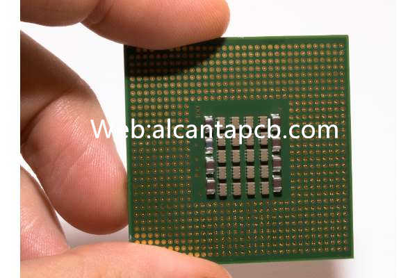
FCBGA (ABF) Substrate Manufacturer
ABF is an advanced substrate material with good dielectric properties and thermal conductivity. Compared with traditional substrate materials, ABF has higher temperature tolerance and mechanical strength, which can meet the requirements for high temperature and high performance. In addition, the lead-free characteristics of ABF substrate materials also meet environmental protection requirements and meet the needs of modern electronic products for environmental protection and sustainable development.
In short, FCBGA (ABF) substrate is an advanced semiconductor device packaging method suitable for high-density electrical connections and excellent electrical performance. The flip chip packaging technology and ABF substrate material used make it widely used in communication equipment, computers and servers, consumer electronics and automotive electronics.
FCBGA (ABF) Substrate design Reference Guide.
FCBGA (Flip Chip Ball Grid Array) substrate is one of the common packaging methods in modern electronic equipment. It uses flip chip packaging technology and uses advanced lead-free solder (ABF) as the substrate material. This design reference guide is designed to provide a comprehensive understanding of FCBGA (ABF) substrate design to help engineers and designers make informed decisions during the design process.
Before starting to design an FCBGA (ABF) substrate, it is important to understand its basic concepts and working principles. This section will introduce the working principle, advantages and common application areas of FCBGA (ABF) substrate.
When designing FCBGA (ABF) substrates, it is crucial to select the appropriate design tools and software. This section will introduce commonly used PCB design software and provide relevant usage tips and precautions.
Selecting the appropriate substrate material is critical to the performance and reliability of FCBGA (ABF) substrates. This section will explore different types of substrate materials, such as FR-4, polyimide, etc., and their advantages and disadvantages in different application scenarios.
Good wiring and layout are key factors in ensuring the performance and reliability of FCBGA (ABF) substrates. This section introduces the basic principles of wiring and layout and provides some suggestions and practical tips.
When designing FCBGA (ABF) substrates, key factors such as signal integrity and electromagnetic compatibility must be considered. This section describes how to optimize layout and design to ensure good signal integrity and immunity to interference.
Effective thermal management is critical to the performance and reliability of FCBGA (ABF) substrates. This section will explore the fundamentals of thermal design and common thermal management techniques such as heat sinks, heat sinks, and heat pipes.
Finally, this section will introduce the production and testing process of FCBGA (ABF) substrate, including manufacturing process, quality control and testing methods.
FCBGA (ABF) substrate design is a complex and precise task that requires the consideration of multiple factors. With the information and guidance provided in this guide, designers can more effectively design and optimize FCBGA (ABF) substrates to meet the requirements of various applications and ensure optimal levels of performance and reliability.
What material is used in FCBGA (ABF) Substrate?
The main material used in FCBGA (ABF) substrates is ABF, which is Advanced Epoxy Mold Compound. ABF is a high-performance epoxy resin composite material with excellent mechanical properties, thermal conductivity and electrical properties, and is suitable for packaging applications of high-density integrated circuits.
The main components of ABF materials include epoxy resin, hardener, fillers and additives. As a basic material, epoxy resin has good adhesion and heat resistance, and can effectively protect chips and circuit components from the external environment. The hardener reacts chemically with the epoxy resin to form a strong network structure, improving the material’s mechanical strength and durability. Fillers are mainly used to adjust the rheological properties and thermal conductivity of materials, as well as enhance the mechanical properties of materials. Additives are used to adjust the hardness, color and other properties of materials to meet the needs of different application scenarios.
During the manufacturing process of FCBGA (ABF) substrates, the ABF material is first laid on the substrate and processed into the required shape and thickness through a specific process. Then, the chip is flipped over and mounted on the substrate, and the chip and the substrate are connected through solder balls to form an electrical connection. Finally, the chip and solder balls on the substrate are encapsulated in ABF material to form a complete packaging structure.
In general, ABF is an ideal packaging material with excellent performance and process characteristics, suitable for packaging applications of high-density integrated circuits, and provides a reliable foundation for the manufacturing of FCBGA (ABF) substrates.
What size are FCBGA (ABF) Substrate?
FCBGA (ABF) substrate sizes vary depending on their application areas and specific designs, allowing different sizes and shapes to be achieved as needed. Generally speaking, the size of the FCBGA (ABF) substrate depends on the following factors:
First, the size of the FCBGA (ABF) substrate is affected by the number and density of chips within it. Larger substrates can accommodate more chips, so in high-performance applications that require the integration of a large number of functional modules, the substrate size may be larger.
Secondly, the application scenario and device size will also affect the size of the FCBGA (ABF) substrate. In consumer electronics such as smartphones, tablets and other small devices, smaller size substrates are often required to accommodate the compact design of the device. On the contrary, in large equipment such as data center servers and network equipment, the substrate size may be larger.
In addition, design requirements and technical limitations also affect the size of the FCBGA (ABF) substrate. For example, achieving higher electrical connection density and better thermal performance may require a more complex multi-layer design or increased substrate thickness, thus affecting the size of the substrate.
In general, the size of FCBGA (ABF) substrates can range from a few millimeters to tens of millimeters, depending on factors such as design requirements, application scenarios, and manufacturing technology. As technology continues to advance and application fields expand, the size range of FCBGA (ABF) substrates is also expanding to meet an increasingly wider range of needs.
The Manufacturer Process of FCBGA (ABF) Substrate.
The manufacturing process of FCBGA (ABF) substrates is a complex and precise process designed to ensure the quality and performance of the final product. The following are the main steps of the manufacturing process of FCBGA (ABF) substrate:
Substrate preparation: The first step in the manufacturing process is to prepare the substrate material. Typically, high-quality Advanced Lead-Free Solder (ABF) is used as the substrate material. ABF material has excellent dielectric properties and thermal conductivity properties, and is suitable for high-density electrical connection requirements.
Flip chip packaging: In the flip chip packaging process, the chip is turned over and placed upside down on the ABF substrate. Then, through precise process control, the chip is accurately connected to the solder balls on the substrate.
Soldering: The next step in connecting the chip to the substrate is soldering. This involves joining the chip and substrate together through a soldering process to ensure a solid electrical connection and good thermal conductivity.
Testing of electrical connections: An important step in the manufacturing process is testing of electrical connections. By using high-precision test equipment, each solder ball connection is tested to ensure that it has a solid connection and good electrical performance.
Cleaning and Inspection: During the final stages of the manufacturing process, FCBGA (ABF) substrates are cleaned and inspected. This includes removing any residue and impurities that may be present and visually inspecting the substrate to ensure there are no defects or damage.
Encapsulation and Packaging: After completing the manufacturing process, the FCBGA (ABF) substrate is encapsulated and packaged for easy transportation and use. The packaging process involves placing the substrate in an appropriate packaging container and adding anti-static materials to protect the substrate from static damage.
By strictly controlling each manufacturing step, the quality and performance of FCBGA (ABF) substrates are ensured to meet expected standards. This precise manufacturing process provides high-performance and reliable chip packaging solutions for various application scenarios, driving the development and innovation of modern electronic technology.
The Application area of FCBGA (ABF) Substrate.
FCBGA (ABF) substrates are widely used in the electronic field. Its high density, excellent electrical performance and adaptability make it the preferred packaging solution in many fields.
First of all, FCBGA (ABF) substrate plays an important role in the field of communication equipment. In communication equipment such as network routers, switches, and base stations, high-performance processors and memory modules are often packaged in FCBGA (ABF) to achieve fast and stable data transmission and processing.
Secondly, FCBGA (ABF) substrates are also widely used in the computer and server fields. In high-performance servers, data centers and supercomputers, processors, graphics chips and memory modules are often packaged in FCBGA (ABF) to meet large-scale data processing and computing needs.
In addition, consumer electronics are also important application areas for FCBGA (ABF) substrates. In consumer electronics products such as smartphones, tablets, TVs, and game consoles, high-performance processors, graphics chips, and memory modules are packaged in FCBGA (ABF) to achieve smooth multimedia experience and efficient application operation.
Finally, the automotive electronics field is also an important application market for FCBGA (ABF) substrates. In automotive electronic control units (ECUs), driving assistance systems and in-vehicle entertainment systems, high-performance processors, sensors and communication modules are packaged in FCBGA (ABF) to achieve vehicle intelligence and improve safety performance.
In general, FCBGA (ABF) substrates have a wide range of applications in the fields of communications, computers, consumer electronics, and automotive electronics. They provide high-performance and high-reliability chip packaging solutions for various application scenarios and promote electronic technology. progress and innovation.
What are the advantages of FCBGA (ABF) Substrate?
FCBGA (ABF) substrates have several advantages that make them an important choice in modern electronic packaging:
High-density connection: The FCBGA (ABF) substrate adopts flip chip packaging technology to achieve high-density electrical connections. The chip and substrate are directly connected through solder balls, which effectively reduces the connection resistance and inductance and improves the signal transmission rate and quality. This high-density connection makes it possible to integrate more functional modules in a limited space, thus enabling more compact and higher-performance electronic product designs.
Excellent electrical properties: ABF (Advanced Lead-Free Solder), as a substrate material, has good dielectric properties and thermal conductivity. This characteristic helps improve the stability and reliability of the circuit and reduces signal attenuation and noise interference in the circuit, thereby ensuring high-quality performance of electronic products.
Strong adaptability: FCBGA (ABF) substrate can adapt to various environmental conditions and operating temperatures, so it performs well in a wide range of application scenarios. Whether in the fields of communication equipment, computers and servers, consumer electronics or automotive electronics, FCBGA (ABF) substrates can play a stable and efficient role.
Space saving: Since the FCBGA (ABF) substrate adopts flip chip packaging technology, the chip can be directly connected to the substrate without using traditional cable connections. This direct connection method not only improves the signal transmission rate, but also saves space, making the overall package more compact, which is conducive to the simplification and lightweight of product design.
Low manufacturing cost: The manufacturing process of FCBGA (ABF) substrate is relatively simple, and the cost of materials used is low, so it has low manufacturing cost. This makes FCBGA (ABF) substrates the first choice for many electronic product manufacturers, helping them reduce the overall cost of their products and improve market competitiveness.
To sum up, FCBGA (ABF) substrate has become an ideal choice in the field of modern electronic packaging due to its many advantages such as high-density connection, excellent electrical performance, strong adaptability, space saving and low manufacturing cost, and has promoted the development of electronic products. Continuous innovation and development.
FAQ
What is FCBGA (ABF) substrate?
FCBGA (ABF) substrate is a semiconductor device packaging method that uses flip chip packaging technology. The key part is advanced lead-free solder (ABF) as the substrate material. This packaging method allows the chip to be directly connected to the solder balls on the substrate, allowing for high-density electrical connections and excellent electrical performance.
In what fields are FCBGA (ABF) substrates widely used?
FCBGA (ABF) substrates are widely used in communication equipment, computers and servers, consumer electronics, and automotive electronics. Among them, high-performance processor packaging in communication equipment, computers and servers, processor and memory packaging in consumer electronics, and automotive electronic control units (ECUs) are its main application areas.
What are the advantages of FCBGA (ABF) substrates?
The advantages of FCBGA (ABF) substrates include high density, excellent electrical performance, direct chip connection, and adaptability. These advantages give it a clear competitive advantage in high-performance and high-reliability chip packaging, and it has been widely used and recognized.
How to choose a suitable FCBGA (ABF) substrate supplier?
Choosing a suitable FCBGA (ABF) substrate supplier requires consideration of the supplier’s technical capabilities, production process, product quality, delivery cycle, and after-sales service. It is recommended to select through market research, supplier evaluation and sample testing to ensure that you select a supplier with stability and reliability.