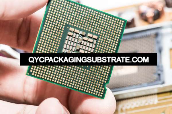
FPGA Package Substrates Manufacturer.An FPGA package substrates manufacturer specializes in producing high-performance substrates for Field-Programmable Gate Arrays (FPGAs). These substrates are critical for ensuring reliable electrical connections and thermal management in FPGA packages. The manufacturer focuses on advanced materials and precision engineering to meet the demands of modern electronics, enabling efficient signal transmission and heat dissipation in complex FPGA designs. Their expertise ensures the delivery of high-quality, custom substrates tailored to the specific needs of FPGA applications.
Field-Programmable Gate Arrays (FPGAs) are highly versatile semiconductor devices that can be configured by the user after manufacturing to perform a wide range of tasks. The substrates used in FPGA packages play a critical role in ensuring the device’s performance, reliability, and integration into electronic systems. This article explores the structure, materials, manufacturing processes, applications, advantages, and frequently asked questions (FAQs) related to FPGA package substrates.
Structure of FPGA Package Substrates
The structure of FPGA package substrates is designed to support high-performance computing and flexible design configurations:
Typically composed of high-performance materials such as organic laminates (e.g., BT epoxy resin or FR-4) or ceramic substrates (e.g., alumina or aluminum nitride).
Multiple layers of copper or other conductive metals are used to create complex interconnects for signal and power distribution.
Insulating layers between conductive layers to ensure electrical isolation and signal integrity.
Dedicated planes within the substrate to distribute power and ground signals efficiently, reducing noise and improving performance.
Vertical interconnects that connect different layers of the substrate, enabling complex routing and high-density designs.
Protective coatings, such as ENIG (Electroless Nickel Immersion Gold) or OSP (Organic Solderability Preservatives), to enhance solderability and protect against oxidation.
Materials Used in FPGA Package Substrates
Key materials used in FPGA package substrates include:
Materials like BT epoxy resin or FR-4 provide good mechanical strength, electrical performance, and cost-effectiveness.
Alumina or aluminum nitride offer superior thermal conductivity and mechanical stability for high-performance applications.
Used extensively for conductive traces and planes due to its excellent electrical conductivity and reliability.

FPGA Package Substrates Manufacturer
High-performance insulating materials, such as polyimides or liquid crystal polymers (LCP), provide electrical isolation and signal integrity.
Coatings like ENIG or OSP protect copper traces from oxidation and enhance solderability for component attachment.
Manufacturing Process of FPGA Package Substrates
The manufacturing process of FPGA package substrates involves several precise steps to ensure quality and performance:
Choosing the appropriate base material and conductive layers based on performance requirements.
Stacking and bonding multiple layers of conductive and dielectric materials under heat and pressure.
Precision drilling to create vias and microvias for vertical interconnections between layers.
Electroplating copper onto the substrate and inside vias to establish electrical connections.
Using photolithography and chemical etching to define the circuit patterns and interconnects.
Applying protective coatings to exposed copper surfaces for enhanced solderability and protection.
Attaching the FPGA die to the substrate using wire bonding or flip-chip technology, followed by encapsulation with molding compounds or protective coatings.
Comprehensive electrical and functional testing to ensure the substrate meets performance specifications and reliability standards.
Applications of FPGA Package Substrates
FPGA package substrates are used in a wide range of applications, including:
Networking equipment, base stations, and data centers where high-speed data processing and flexible configuration are required.
Devices like smartphones, tablets, and gaming consoles that demand high performance and adaptability.
Advanced driver-assistance systems (ADAS), infotainment systems, and engine control units (ECUs) in modern vehicles.
Applications such as radar systems, avionics, and communication equipment where reliability and performance are critical.
Robotics, control systems, and IoT devices in manufacturing and process control environments.
Advantages of FPGA Package Substrates
FPGA package substrates offer several significant advantages:
Support for complex interconnects and high-speed signal transmission, essential for advanced computing tasks.
Ability to reconfigure and adapt to different functions and applications, providing versatility in design.
Efficient heat dissipation through substrate materials and design features, ensuring reliable operation under high-power conditions.
Robust construction and testing ensure long-term performance in demanding environments.
Facilitate the integration of FPGAs into various electronic systems, enhancing overall device functionality.
FAQ
What materials are typically used for FPGA package substrates, and why?
FPGA package substrates commonly use materials like organic laminates (BT epoxy resin, FR-4) for their cost-effectiveness and good electrical properties, and ceramic substrates (alumina, aluminum nitride) for their superior thermal conductivity and mechanical stability.
How do FPGA package substrates contribute to the performance of electronic devices?
FPGA package substrates enhance device performance by providing efficient power distribution, high-speed signal transmission, and effective thermal management, all of which are critical for advanced computing and high-performance applications.
In which industries are FPGA package substrates most commonly used?
FPGA package substrates are widely used in telecommunications, consumer electronics, automotive electronics, aerospace and defense, and industrial automation due to their high performance, flexibility, and reliability.
What are the key manufacturing steps for FPGA package substrates to ensure quality and reliability?
Key manufacturing steps include material selection, lamination, drilling and via formation, copper plating, patterning and etching, surface finish application, assembly, and comprehensive testing to ensure quality, reliability, and adherence to performance specifications.
 Professional Flip-Chip Packaging Substrate Supplier
