 Professional Flip-Chip Packaging Substrate Supplier

High Frequency Printed Circuit Board Manufacturer.As a leading High Frequency Printed Circuit Board Manufacturer, we specialize in creating advanced PCBs that cater to the demands of high-speed, high-frequency applications. Our state-of-the-art manufacturing processes ensure superior signal integrity and thermal performance, making our products ideal for telecommunications, aerospace, and cutting-edge computing technologies. Trust us for innovative solutions that drive the future of high-frequency electronics.
High Frequency Printed Circuit Boards (HF PCBs) are a critical component in modern electronics, designed to operate at high frequencies, typically above 1 GHz. These boards are essential in applications requiring fast signal transmission, minimal signal loss, and precise signal integrity. HF PCBs are widely used in telecommunications, aerospace, military, and advanced computing systems. This article explores the properties, structure, materials, manufacturing process, applications, and advantages of High Frequency Printed Circuit Boards.
What is a High Frequency Printed Circuit Board?
A High Frequency Printed Circuit Board (HF PCB) is a specialized type of PCB designed to handle high-frequency signals with minimal interference and signal loss. HF PCBs are crucial for applications that require rapid data transmission and high signal fidelity. These boards are engineered with materials and design techniques that ensure reliable performance at high frequencies.
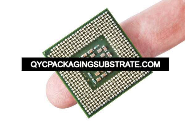
High Frequency Printed Circuit Board Manufacturer
HF PCBs differ from standard PCBs primarily in their material composition and design. They use low-loss materials with stable dielectric properties to maintain signal integrity. The design of HF PCBs involves careful consideration of trace geometry, layer stacking, and impedance control to minimize signal degradation and electromagnetic interference (EMI).
Structure of High Frequency Printed Circuit Boards
The structure of High Frequency Printed Circuit Boards is designed to support high-speed signal transmission while maintaining signal integrity and minimizing loss. Key structural elements include:
The substrate material in HF PCBs is typically made from low-loss laminates with stable dielectric properties. These materials are crucial for minimizing signal attenuation and maintaining signal integrity at high frequencies.
The signal layers in HF PCBs are carefully designed to optimize trace geometry and minimize signal loss. Techniques such as controlled impedance routing and differential pair routing are employed to ensure precise signal transmission.
HF PCBs often include dedicated ground and power planes to reduce EMI and provide stable reference voltages. These planes help maintain signal integrity by providing a continuous return path for high-frequency signals.
Vias in HF PCBs are designed to minimize signal reflection and loss. Techniques such as back drilling and blind/buried vias are used to optimize via performance at high frequencies.
The surface finish on HF PCBs is selected to enhance solderability and protect against oxidation. Common finishes include ENIG (Electroless Nickel Immersion Gold) and immersion silver.
Materials Used in High Frequency Printed Circuit Boards
The materials used in High Frequency Printed Circuit Boards are chosen for their ability to support high-speed signal transmission with minimal loss and interference. Key materials include:
Materials such as PTFE (polytetrafluoroethylene), Rogers, and ceramic-filled laminates are commonly used in HF PCBs. These materials have low dielectric constants (Dk) and low dissipation factors (Df), which help maintain signal integrity and reduce signal loss.
High-quality copper foil is used for the signal layers, power planes, and ground planes. Copper offers excellent electrical conductivity, essential for high-speed data transmission. The copper foil is typically applied using techniques such as electroplating and etching to achieve precise results.
Prepreg materials, which are resin-coated fiberglass sheets, are used to bond the layers of the HF PCB together. These materials provide electrical insulation and mechanical strength, ensuring the board can withstand the stresses of high-frequency operation.
Effective thermal management is crucial in HF PCBs to prevent overheating and ensure reliable performance. Materials with high thermal conductivity, such as thermal interface materials (TIMs), are used to dissipate heat efficiently.
The Manufacturing Process of High Frequency Printed Circuit Boards
The manufacturing process of High Frequency Printed Circuit Boards involves several precise steps to ensure high performance and reliability. The process includes:
High-quality, low-loss laminates and copper foils are prepared. The materials are selected based on their dielectric properties and ability to support high-frequency signals.
The core material is laminated with copper foils to form the initial substrate. Multiple layers of prepreg and copper are then stacked and bonded together using a lamination process. Precise alignment and control are crucial to ensure that the layers are properly registered and bonded.
Holes are drilled into the substrate to create vias and through-holes. Advanced drilling techniques, such as laser drilling, are used to achieve the high precision required for HF PCBs.
The drilled holes are plated with copper to create electrical connections between the layers. This involves depositing a thin layer of copper onto the walls of the holes using electroplating techniques. The plating process must be carefully controlled to ensure uniform coverage and adhesion.
The desired circuit patterns are transferred onto the copper layers using a photolithographic process. This involves applying a photosensitive film (photoresist) to the copper surface and exposing it to ultraviolet (UV) light through a photomask. The exposed areas of the photoresist are developed, leaving behind the circuit pattern. The board is then etched to remove the unwanted copper, leaving only the circuit traces.
A solder mask is applied to the board to protect the circuitry and prevent solder bridges during assembly. The solder mask is typically applied using screen printing or photo-imaging techniques and then cured to harden it.
A surface finish is applied to the exposed copper areas to enhance solderability and protect against oxidation. Common surface finishes include Electroless Nickel Immersion Gold (ENIG), Hot Air Solder Leveling (HASL), and Immersion Silver.
The board is assembled with electronic components, such as integrated circuits (ICs), resistors, capacitors, and connectors. This step involves placing the components onto the board and soldering them in place using reflow soldering or wave soldering techniques.
The final step involves rigorous testing and inspection to ensure the board meets all performance and reliability requirements. Electrical testing, visual inspection, and automated optical inspection (AOI) are used to identify any defects or irregularities. Any issues identified during testing are addressed before the boards are approved for shipment.
The manufacturing process of HF PCBs requires precise control and expertise to ensure high quality and reliability. Each step is critical for achieving the desired performance and reliability of the final product.
Application Areas of High Frequency Printed Circuit Boards
High Frequency Printed Circuit Boards are used in a wide range of applications across various industries due to their ability to handle high-speed signal transmission with minimal loss and interference. Key application areas include:
HF PCBs are widely used in telecommunications equipment, such as routers, switches, and base stations, where high-speed data transmission and signal integrity are critical.
The aerospace and defense industries use HF PCBs in radar systems, satellite communications, and avionics. These applications require reliable high-frequency performance in demanding environments.
In the automotive industry, HF PCBs are used in advanced driver-assistance systems (ADAS), infotainment systems, and vehicle-to-everything (V2X) communication systems. These applications require high-speed data transmission and reliable performance.
HF PCBs are used in medical devices, such as imaging equipment and diagnostic instruments, where precise signal transmission and reliability are essential.
HF PCBs are used in high-speed computing systems, such as servers and supercomputers, where fast data processing and signal integrity are critical for performance.
Advantages of High Frequency Printed Circuit Boards
High Frequency Printed Circuit Boards offer several advantages that make them a preferred choice for high-speed and high-reliability applications. These advantages include:
HF PCBs are designed to minimize signal loss and distortion, ensuring high-speed data transmission with minimal interference. The use of low-loss materials and advanced routing techniques helps maintain signal integrity and reduce electromagnetic interference (EMI).
Effective thermal management is critical for high-speed applications. HF PCBs incorporate advanced thermal interface materials and optimized structures to dissipate heat efficiently, preventing performance degradation due to overheating.
The robust construction and high-quality materials used in HF PCBs ensure reliable performance in demanding applications. These boards are designed to withstand thermal cycling, mechanical stress, and harsh environmental conditions, making them suitable for use in critical applications.
HF PCBs are versatile and can be used in a wide range of applications, from telecommunications and aerospace to high-speed computing and automotive electronics. The combination of high performance, reliability, and scalability makes these PCBs an ideal choice for various industries and applications.
FAQ
What makes High Frequency Printed Circuit Boards suitable for high-speed applications?
High Frequency Printed Circuit Boards are designed with advanced materials and manufacturing techniques that ensure minimal signal loss, low electromagnetic interference (EMI), and robust performance under high-speed conditions. The use of low-loss laminates, precise signal routing, and effective thermal management solutions makes these PCBs ideal for handling data rates above 1 GHz.
Can High Frequency Printed Circuit Boards be used in harsh environments?
Yes, High Frequency Printed Circuit Boards are highly suitable for use in harsh environments. The robust structure, high-quality materials, and advanced manufacturing processes ensure reliable performance under varying environmental conditions, such as high temperatures, humidity, and mechanical stress. This makes them ideal for applications in aerospace, defense, and automotive electronics.
How do High Frequency Printed Circuit Boards ensure effective thermal management?
High Frequency Printed Circuit Boards incorporate advanced thermal interface materials and optimized structures to dissipate heat efficiently. The use of materials with high thermal conductivity and effective heat dissipation techniques ensures that critical components are kept within safe operating temperatures, preventing performance degradation due to overheating.
What industries benefit the most from using High Frequency Printed Circuit Boards?
Industries that benefit the most from using High Frequency Printed Circuit Boards include telecommunications, aerospace, defense, automotive electronics, medical devices, and high-speed computing. These industries require high-speed data transmission, minimal signal loss, and reliable performance, all of which are provided by HF PCBs.