 Professional Flip-Chip Packaging Substrate Supplier

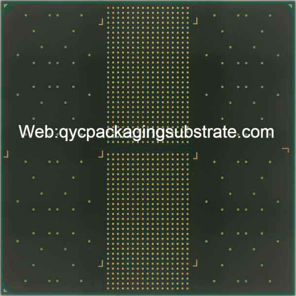
High precision packaging substrate Manufacturer. We use the mSap and Sap Advanced production technology to produce the Package Substrate. and the packaging substrate will be made with BT, and Showa Denko and Ajinomoto base materials. or other types High speed materials, or maybe high frequency materials.
This passage emphasizes the crucial role of high-precision packaging substrates in electronic equipment. These substrates, typically constructed from insulating materials such as fiberglass reinforced epoxy (FR-4) with a conductive copper surface, serve as essential platforms for both physical and electrical connections within electronic devices. They are instrumental in facilitating the connection and support of various electronic components, including integrated circuits (ICs) and transistors. The design and manufacturing processes adhere to stringent standards to ensure the performance, reliability, and stability of electronic devices.
High-precision packaging substrates contribute significantly to efficient signal transmission, thermal management, and circuit layout, thereby ensuring the stable operation and optimal performance of electronic devices. In addition to facilitating electrical connections, they also efficiently conduct heat, aiding in maintaining an appropriate operating temperature for electronic devices. With a high level of density and precision, these substrates enable the fulfillment of complex circuit routing requirements and can be customized in various shapes and sizes to meet diverse application scenarios.
In summary, high-precision packaging substrates are integral components in electronic devices, providing essential platforms for connections and support. Their adherence to stringent standards and processes underscores their role in ensuring the performance and reliability of electronic devices, contributing significantly to the development and progress of modern technology.
High precision packaging substrate Manufacturer
What types of high-precision packaging substrates are there?
This passage discusses various types of high-precision packaging substrates in the electronics industry, focusing on single-sided and double-sided PCBs. Single-sided PCBs are described as simple substrates with circuitry on one side and often a copper foil or overlay on the other side, suitable for low-complexity applications due to their lower wiring complexity and cost. On the other hand, double-sided PCBs are highlighted for having circuitry on both sides, allowing for higher wiring density and better performance. They find widespread use in moderately complex electronic products such as computer peripherals and consumer electronics, offering improved electrical connections and greater connectivity.
This passage discusses various types of high-precision packaging substrates commonly utilized in electronic circuitry:
Multi-layer Printed Circuit Boards (PCBs): These circuitry panels feature multiple internal tiers, allowing for increased wiring density and enhanced signal integrity. They are utilized in contexts demanding high-density and high-speed performance, such as telecommunications equipment and computer mainboards, effectively reducing electromagnetic interference and signal interference.
Rigid-Flex PCBs: These circuit boards integrate inflexible substrates with adaptable wiring, making them suitable for confined environments or applications necessitating flexibility, such as handheld electronics and automotive systems. They ensure reliable electrical connections while providing robust mechanical resilience and adaptability.
High-frequency Packaging Substrates (High-frequency PCBs: Engineered specifically for precise signal transmission and interference mitigation in domains like radio frequency apparatus and satellite communications, these substrates employ specialized materials and processes to ensure stability and reliability.
High-speed Digital PCBs: Customized to fulfill the demands of high-speed data transmission and processing in areas like computer networks and data centers, these substrates boast exceptional signal integrity and interference resistance achieved through specialized wiring designs and inter-layer connectivity technologies.
The passage highlights that each type of substrate has distinct characteristics and applications, offering the flexibility for selection and customization to meet specific performance and reliability requirements.
What are the advantages of high-precision packaging substrates?
This paragraph outlines the benefits of high-precision packaging substrates in comparison to other circuit boards. These substrates offer numerous advantages that can enhance the performance and reliability of electronic products.
First, the high-precision packaging substrate provides highly reliable electrical connections. Through precise design and manufacturing, packaging substrates ensure stable connections between electronic components, reducing the risk of disconnection or circuit breakage, thereby improving circuit stability and reliability.
This passage discusses the advantages of high-precision packaging substrates in modern electronic products. It highlights several key benefits:
This passage highlights the importance of high thermal conductivity in advanced packaging substrates, especially for electronic devices with heightened component integration and power density. Efficient heat dissipation is vital for preventing overheating and safeguarding components, thereby ensuring optimal device performance.
High-Density Integration and Miniaturized Designs: These substrates facilitate compact layouts of electronic components, allowing for high circuit integration and product miniaturization. This feature meets the demand for smaller, lighter electronic products while maintaining performance.
Suitability for Complex Circuit Wiring: The manufacturing process enables precise circuit layouts and intricate connections, accommodating diverse circuit wiring requirements. This capability enhances product performance and functionality by meeting specific electronic product needs.
Overall, high-precision packaging substrates offer stable electrical connections, superior thermal conductivity, high integration density, miniaturization potential, and compatibility with complex circuitry. These advantages collectively enhance electronic product performance, reliability, and meet diverse packaging substrate needs across various industries.
Why choose high-precision packaging substrate?
This passage discusses the advantages of High Precision Packaging Substrate (HPPS) in electronic component selection. It highlights three main advantages:
Excellent Electrical Connection Performance: HPPS ensures stable and reliable electrical connections, crucial for data transmission and signal conduction in modern electronic devices.
Superior Thermal Conductivity: HPPS effectively dissipates heat generated by electronic equipment during operation, maintaining normal operating temperatures and enhancing device stability and long-term reliability.
Support for High-Density Integration and Miniaturized Design: HPPS facilitates high-density integration through optimized design and layout, accommodating more components in limited spaces while maintaining a compact design, thus enhancing the overall performance of electronic devices.
In addition, high-precision packaging substrates are suitable for complex circuit wiring requirements. Modern electronic equipment often has complex circuit structures and wiring requirements, requiring effective layout of multiple circuits in a limited space. High-precision packaging substrates use advanced processes and technologies to meet the requirements of complex circuit wiring and provide efficient and reliable solutions.
In summary, the benefits of employing high-precision packaging substrates in numerous electronic components are evident. These substrates not only ensure dependable electrical connections and superior thermal conductivity but also facilitate high-density integration and miniaturized design, effectively meeting the escalating requirements for performance and reliability in contemporary electronic devices. Consequently, opting for high-precision packaging substrates stands as a prudent decision to enhance the performance and reliability of electronic equipment.
How to manufacture high-precision packaging substrates?
This passage outlines the detailed manufacturing process of high-precision packaging substrates and the key steps involved:
This passage outlines the initial stages of electronic circuit board production. Firstly, the motherboard, typically composed of fiberglass reinforced epoxy (FR-4), acts as the substrate carrier. Substrates, insulated materials with copper foil coatings, support and connect electronic components.
Following this, in the lamination process, various substrate materials are stacked and subjected to elevated temperatures and pressures. This process fuses them together into a cohesive unit, ensuring adherence to thickness and size requirements. Additionally, it establishes a strong bond between the copper foil and insulating layers, guaranteeing dependable electrical connections.
Drilling is a pivotal phase in high-precision packaging substrate manufacturing. Here, precision CNC drilling machines are employed to bore holes into the substrate, creating pathways for circuit routing and component mounting.
Following drilling, electroless copper plating is conducted. This process chemically deposits a copper layer onto the inner walls and hole surfaces of the substrate, enhancing conductivity and connectivity.
This passage describes the process of circuit pattern formation on substrates through patterned etching and the subsequent component mounting onto the substrate. Initially, photosensitive adhesive is applied to the substrate surface, followed by exposure to ultraviolet light to create the desired circuit pattern. Excess copper foil is then removed through development and etching. In the final stage, components such as chips, resistors, and capacitors are precisely soldered onto designated locations on the substrate. Subsequently, soldering, inspection, and testing are performed to ensure the performance and reliability of electronic products.
Through these key steps, high-precision packaging substrates are manufactured, offering a solid foundation and dependable support for the optimal functioning of various electronic devices.
What are the application areas of high-precision packaging substrates?
This passage highlights the significance of high-precision packaging substrates in modern electronic equipment across various industries, particularly in communications and automotive electronics.
This passage highlights the significance of high-precision packaging substrates in various industries, particularly in communications and automotive electronics. These substrates serve as crucial elements in facilitating the connection and support of diverse communication equipment and automotive systems, ensuring efficient performance, reliability, and safety. They enable high-speed data transmission, signal processing, and modulation/demodulation functions in communication systems, while also withstanding harsh environmental conditions in automotive applications. Additionally, they find use in medical devices for accurate data collection and processing, as well as in industrial control for enhancing production efficiency and safety. Overall, high-precision packaging substrates play a critical role in the performance and reliability of electronic devices across multiple industries, with their importance expected to increase further with technological advancements and expanded application areas, driving development and innovation.
How to find a high-quality packaging substrate manufacturer?
This passage emphasizes the crucial factors to consider when searching for a high-quality packaging substrate manufacturer. It underscores the importance of assessing the supplier’s technical strength, including advanced production equipment and professional teams. Additionally, a robust quality management system is highlighted as essential to ensure products meet specifications. Experience and reputation are emphasized to mitigate cooperation risks, while customer service, including timely response and support, is deemed vital.
When selecting a partner, the advice is to conduct a comprehensive evaluation based on the company’s specific needs. This involves confirming that the supplier aligns with technical requirements and production capacity, meets delivery timelines, and offers fair pricing, which should be considered alongside product quality and service levels. The passage also stresses the significance of establishing a positive and long-term cooperative relationship with suppliers who share the company’s culture and values for stable and reliable support in business development.
In summary, identifying a top-tier packaging substrate manufacturer entails evaluating aspects like technical expertise, quality assurance practices, industry experience, reputation, and level of customer support. The selection process should be tailored to the specific requirements of the company, emphasizing the establishment of a robust and lasting partnership for shared success.
What is the quotation for high-precision packaging substrates?
This paragraph discusses the importance of high-precision packaging substrates in electronic manufacturing and outlines key factors influencing their quotation.
Material Cost: The cost of packaging substrates depends on various materials involved such as substrate materials, conductor materials, and insulating materials. Discrepancies in material selection directly impact the final quotation.
Process Complexity: Manufacturing high-precision packaging substrates necessitates advanced processes and equipment. More intricate processes tend to escalate manufacturing costs, which are reflected in the quotation.
Quantity Requirements: Typically, larger quantities result in lower unit prices. Bulk orders often offer better cost-effectiveness, whereas low-volume production may escalate the cost per substrate.
Technical requirements: Some special technical requirements, such as specific laminate structures, fine lines, high-density wiring, etc., may increase manufacturing difficulty and cost.
Lead time: Urgent orders or situations requiring quick delivery may result in rush production, thereby increasing manufacturing costs.
How to communicate with the manufacturer to obtain detailed quotation information?
This paragraph outlines the steps involved in effectively communicating with a manufacturer to ensure the production of high-quality packaging substrates:
Clarify Requirements: Before engaging with the manufacturer, it’s crucial to establish clear specifications for the product, including size, material, layer count, surface treatment, etc.
Provide Detailed Design Information: Furnish the manufacturer with comprehensive design documents such as Gerber files, layout drawings, and laminate structures to enable accurate cost evaluation.
Request Quotation Details: Ask the manufacturer for a breakdown of the quotation, including material costs, processing costs, sampling costs, and transportation expenses, to ensure full understanding.
Discuss Mass Production Plan: For mass production, engage in discussions with the manufacturer regarding the production plan to explore potential cost-saving arrangements.
Understand Payment Terms: Thoroughly comprehend the payment terms outlined in the quotation, including down payment requirements and final payment deadlines, to avoid any misunderstandings during the transaction.
Full Communication and Selection: Engage in open communication with the manufacturer and carefully assess the quotation plans to choose the option that aligns best with your requirements and budget constraints, ensuring the production of high-quality and precise packaging substrates.
Frequently Asked Questions
Why should I choose high precision packaging substrates over other boards?
High precision packaging substrates offer superior performance and reliability, especially in applications that demand circuit stability and high-speed transmission, such as communication devices, computers, and medical equipment.
How are high precision packaging substrates manufactured?
The manufacturing process of high precision packaging substrates includes fabrication of the motherboard and substrate, lamination, drilling, copper plating, graphic etching, and assembly. Strict process control and precision equipment ensure product quality.
How are prices quoted for high precision packaging substrates?
The pricing of high precision packaging substrates depends on factors such as materials, processes, complexity, and quantity. Direct communication with manufacturers to obtain detailed pricing information is advised.
What are some common questions regarding high precision packaging substrates?
Common questions about high precision packaging substrates include queries about material selection, process flow, technical support, and more. Understanding these questions and their answers can help readers gain a better understanding and make informed decisions when selecting packaging substrate products.
What are some common questions and concerns regarding high precision packaging substrates?
Common questions include those related to material selection, the manufacturing process, technical support, and specific application requirements. Addressing these concerns helps readers gain a better understanding and make informed choices when selecting packaging substrate products.