 Professional Flip-Chip Packaging Substrate Supplier

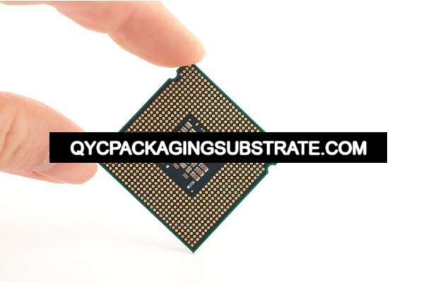
High Speed package Substrate Manufacturer. High Speed material has BT series materials, ABF series materials. We use advanced Msap and Sap technology to manufacture the High multilayer interconnection High Speed substrates from 2 to 20 layers.
The passage discusses the importance of high-speed packaging substrates in electronic communications. These substrates are crucial for transmitting high-frequency, high-speed signals reliably. They are crafted using specialized materials and processes to ensure stability and minimize signal transmission losses, thereby enhancing signal integrity for accurate data transmission.
Additionally, high-speed packaging substrates possess exceptional anti-interference capabilities, allowing them to withstand external electromagnetic interference and noise. This feature enables stable signal transmission in complex electromagnetic environments, ensuring the normal functioning of electronic equipment.
Moreover, these substrates have higher density and smaller size, making them suitable for contemporary electronic devices with volume and weight constraints. As a result, they are widely used in compact products like mobile phones, laptops, and communication equipment.
High Speed package Substrate Manufacturer
In summary, high-speed packaging substrates are indispensable components characterized by high-frequency capabilities, exceptional anti-interference performance, and a compact size. They play a pivotal role in supporting the performance enhancement and size reduction of modern electronic communication equipment.
What are the types of high-speed packaging substrates?
High-speed packaging substrates play a crucial role in modern electronic devices, offering diverse options tailored to specific needs. Here’s a closer look:
HDI (High-Density Interconnect) boards enhance circuit board wiring density by incorporating more wiring on the same layer. Utilizing technologies like microvias, blind vias, and buried vias, HDI boards feature multi-layer structures, enabling compact layouts and heightened signal density. Ideal for high-speed signal transmission and intricate circuit designs.
Rigid-Flex boards combine rigid and flexible components, offering both flexibility and durability. These composite boards, comprising stacked rigid and flexible panels, are adept at applications requiring bending or folding, such as mobile devices and medical equipment, where space constraints or reliability are paramount.
High-speed backplanes serve as connectors for multiple electronic devices, commonly found in network equipment, servers, and data storage systems. These boards boast larger sizes and higher signal transmission rates, necessitating considerations like signal integrity and interference mitigation. They often employ high-performance materials and complex lamination processes to meet rigorous demands.
Packaging substrates are utilized for packaging chips and electronic devices, typically for integrated circuit packaging. Renowned for their high density and performance, they facilitate chip-scale and system-level packaging, offering swift signal transmission rates and reduced power consumption, integral for contemporary electronic products.
High-speed interconnect boards excel in transmitting high-speed signals, commonly deployed in data centers and communication equipment. Renowned for superior signal integrity and anti-interference capabilities, these boards support complex circuit designs and high-speed data transmission, crucial for demanding applications.
Selecting the right high-speed packaging substrate is paramount for electronic product performance and reliability, necessitating careful consideration of application-specific needs and technical requirements during selection and design.
What are the advantages of high-speed packaging substrates over traditional substrates?
High-speed packaging substrates are increasingly favored over traditional substrates in the modern electronics industry due to several distinct advantages. Firstly, they boast superior signal transmission speeds and reduced signal losses. With electronic products demanding higher transmission rates, conventional substrates fall short, whereas high-speed packaging substrates utilize advanced materials and processes to enhance signal transmission speed, minimize loss, and ensure swift data transfer for efficient operation.
Secondly, high-speed packaging substrates exhibit enhanced anti-interference capabilities. Given the complex electromagnetic environments faced by modern electronic devices, particularly mobile and communication devices, there’s a critical need for interference resistance. These substrates leverage premium materials and design features to effectively suppress interference signals, ensuring system stability and boosting product reliability.
Furthermore, high-speed packaging substrates offer heightened levels of integration and reduced form factors. With a prevailing trend toward miniaturization in electronic products, there is an escalating demand for on-board devices to be more compact and seamlessly integrated. By capitalizing on advanced packaging technologies and miniaturization designs, these substrates achieve elevated integration levels and smaller footprints, resulting in products that are both lightweight and streamlined.
To recap, high-speed packaging substrates surpass their traditional counterparts due to their superior signal transmission speeds, minimized signal loss, fortified anti-interference capabilities, heightened integration levels, and diminished form factors. As a result, in today’s intricate and demanding landscape of electronic applications, the preference for high-speed packaging substrates is becoming increasingly prevalent among electronic manufacturers and designers.
Why choose high-speed packaging substrate?
High-speed packaging substrates are highly favored in today’s electronics industry due to their versatility and numerous advantages, making them a top choice across various sectors. Let’s explore why high-speed packaging substrates are preferred and where they find extensive applications.
High-speed packaging substrates are pivotal within the realm of communications, particularly amidst the swift evolution of 5G technology. The escalating need for swift and high-frequency signal transmission underscores their significance. These substrates boast unparalleled signal integrity and interference shielding capabilities, rendering them optimal for 5G base stations, communication apparatus, and analogous uses.
Moreover, the medical domain extensively relies on high-speed packaging substrates. Medical equipment demands real-time, accurate data transmission, which these substrates adeptly fulfill. Whether it’s medical imaging devices or laser surgery systems, the stability and reliability ensured by high-speed packaging substrates are indispensable for seamless operation.
High-speed packaging substrates offer significant benefits to automotive electronics, playing a crucial role in modern vehicles’ electronic systems such as in-car entertainment and driver assistance features. These substrates facilitate swift and reliable data transmission, enhancing the intelligence and safety of automobiles and ultimately elevating the driving experience.
The widespread embrace of high-speed packaging substrates stems from their outstanding performance and reliability across diverse industries. Whether in telecommunications, healthcare, automotive, or other sectors, choosing these substrates offers significant benefits, enhancing product performance and competitiveness in the market. Consequently, manufacturers striving to deliver top-notch electronic products prioritize high-speed packaging substrates as an indispensable option.
What is the manufacturing process of high-speed packaging substrates?
The production process of high-speed packaging substrates is a meticulous and complex procedure designed to guarantee optimal signal transmission performance and stability in the finished product. Here’s a breakdown of the essential steps involved:
Design and Planning: The engineering team starts the process by creating the substrate’s structure and layout based on customer requirements and technical specifications.
Material Selection: Critical to the process is the selection of materials with superior dielectric and high-frequency properties, such as FR-4, PTFE, etc.
Printed Circuit Board (PCB) Manufacturing: This core step involves cutting the substrate material to shape, employing chemical etching or mechanical processing, and applying a conductive layer and printed circuit pattern.
Stacking and Lamination: High-speed packaging substrates often utilize multi-layer stacking for enhanced signal transmission and electromagnetic compatibility. Boards are stacked and laminated under high temperature and pressure.
Drilling and Socket Installation: Holes are drilled at appropriate locations to facilitate circuit connection, assembly, and heat dissipation.
Wiring and Connection: Following stacking and lamination, wiring and connection processes, including soldering and metallization, ensure stable and reliable circuit connections.
Surface treatment methods like tin, lead, or gold spraying are employed to improve conductivity and resist corrosion. Rigorous inspection and testing procedures, including visual assessments, dimensional measurements, and electrical performance tests, ensure compliance with customer specifications and industry standards. Through meticulous adherence to these steps and the implementation of strict quality control measures, high-speed packaging substrates with outstanding performance and reliability are produced, contributing to the progress of the electronics sector.
In what fields are high-speed packaging substrates used?
High-speed packaging substrates are extensively employed across diverse sectors within the electronics industry due to their exceptional performance and reliability. They are particularly favored in several critical domains:
5G Technology: High-speed packaging substrates find extensive usage in 5G base stations and communication equipment. These substrates facilitate high-speed data transmission and frequent signal exchange, ensuring the stability and efficacy of communication systems driven by 5G technology.
High-speed packaging substrates play a critical role across various industries, including medical device manufacturing, aerospace, automotive electronics, and industrial automation. In medical device manufacturing, they enable swift and precise data transmission for equipment like medical imaging devices and patient monitors. Likewise, in aerospace applications, these substrates are indispensable for maintaining high performance and reliability in flight control, navigation, and communication systems. Automotive electronics also leverage their use in entertainment, communication, and autonomous driving technologies, thereby improving vehicle intelligence and safety.In industrial automation, high-speed packaging substrates support control systems, sensor networks, and data acquisition, enabling swift and stable data processing. Overall, their superior performance, reliability, and stability make them indispensable across these industries, with promising future prospects fueled by ongoing technological advancements and expanding applications.
How to obtain high-speed packaging substrate?
Market Research: Conduct thorough market research to identify high-speed packaging substrate manufacturers. Utilize online resources, attend industry exhibitions, and consult with professionals to gain insights into the available options.
Technical Capabilities:Familiarize yourself with the technical and research and development (R&D) capabilities of the supplier. Ensure they utilize advanced production technologies capable of meeting specific demands for high-speed packaging substrates and are up-to-date with industry advancements.
Cooperation History and Cases: Evaluate the supplier’s cooperation history and successful cases to gauge their experience and ability to collaborate with customers. Request samples or references from existing clients to assess product quality and service levels.
Price and Delivery Time:Delve into a comprehensive evaluation of price and delivery time considerations. Foster transparent communication with potential suppliers to negotiate agreements on pricing, delivery schedules, and other pertinent terms, ensuring a seamless and efficient collaboration.
In summary, the process of identifying a dependable high-speed packaging substrate manufacturer entails thorough market research, scrutinizing supplier backgrounds, verifying quality certifications, evaluating technical capabilities, reviewing past collaboration history, and meticulously weighing pricing and delivery timelines. Building a strong partnership with fitting suppliers not only enhances product quality but also elevates the company’s market competitiveness.
What is the quotation for high-speed packaging substrates?
The pricing of high-speed packaging substrates is a crucial aspect that deeply connects manufacturers and customers. Grasping the elements influencing this pricing and mastering the art of acquiring precise quotes are pivotal for efficient budgeting and streamlining production processes.
Firstly, let’s delve into the factors influencing the pricing of high-speed packaging substrates.
Material Choice: Material selection plays a pivotal role in determining the cost of manufacturing high-speed packaging substrates. The choice of materials directly impacts the overall expenses incurred. Opting for high-performance or specialized materials typically commands a higher price tag, albeit offering superior performance characteristics.
Design complexity: The design complexity of the substrate is another important factor. Complex designs may require more layers and higher levels of technology, resulting in higher manufacturing costs.
Production quantity: The production quantity is also directly related to the quotation. High-volume production often enjoys economies of scale, reducing manufacturing costs per substrate.
Technical requirements: If the substrate needs to meet special technical standards or has other customization requirements, this will also have an impact on the quotation.
Communicate directly with manufacturers: Communicating directly with high-speed packaging substrate manufacturers is the first way to obtain accurate quotes. By describing project needs in detail, manufacturers are able to provide professional quotes and recommendations.
Consider technical support: Some manufacturers may offer technical support services to help optimize designs to reduce costs. This is also something worth considering when getting a quote.
When choosing how to obtain a quote, clients need to weigh accuracy against cost. Communicating directly with the manufacturer often results in a more accurate quote and can also establish a long-term relationship to ensure the success of the project.
The quotation of high-speed packaging substrates is a complex and critical issue involving many factors. By understanding the influencing factors behind a quote and choosing the appropriate route to obtain a quote, customers can better plan their budget and ensure the smooth progress of the project. In this highly competitive electronics industry, accurate quotation is not only related to cost control, but also related to the performance and reliability of the final product.
What common questions need to be answered about high-speed packaging substrates?
What factors affect the impedance matching of high-speed package substrates?
Impedance matching ensures efficient signal transfer between components. Factors such as trace geometry, dielectric properties, and termination methods influence impedance matching in high-speed package substrates.
Are there any compatibility concerns when integrating high-speed package substrates with other system components?
Compatibility issues may arise when integrating high-speed package substrates with connectors, components, or PCB assemblies. Ensuring proper interface design and compatibility testing can address these concerns.
What is the impact of via design on signal integrity in high-speed package substrates?
Via design plays a crucial role in signal integrity. Improper via placement or inadequate via structures can introduce signal degradation, impedance mismatch, and EMI issues.
What are the common challenges in manufacturing high-speed package substrates?
High-speed package substrate manufacturing involves intricate processes that may face challenges such as ensuring signal integrity, controlling impedance, and managing thermal issues.
How do I select the right high-speed package substrate for my application?
Choosing the appropriate high-speed package substrate requires considering factors like signal frequency, transmission speed, environmental conditions, and reliability requirements.
What are the common challenges in manufacturing high-speed package substrates?
High-speed package substrate manufacturing involves intricate processes that may face challenges such as ensuring signal integrity, controlling impedance, and managing thermal issues.