 Professional Flip-Chip Packaging Substrate Supplier

IC Substrate Firm. the Package Substrate will be made with Showa Denko and Ajinomoto High speed materials.or other types high speed materials.
In today’s electronic field where technology is changing with each passing day, IC Substrate (integrated circuit substrate) plays an indispensable role. IC Substrate is a specially designed substrate whose main task is to provide support and connections for integrated circuit chips. Let’s take a closer look at what IC Substrate is and how it serves as a substrate to carry integrated circuit chips.
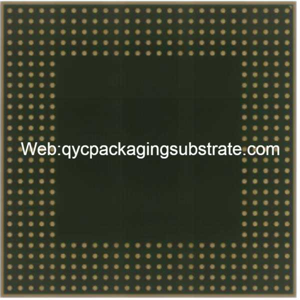
IC Substrate is a multi-layered substrate with a complex structure specifically designed to connect and support integrated circuit chips. This substrate is not only a support structure for electronic devices, but also an important medium for electrical connections in integrated circuits. Through precision design and manufacturing, IC Substrate provides the necessary electrical connections to the chip and provides stable mechanical support in a small space.
The main function of IC Substrate is to carry and connect integrated circuit chips. Its multi-layered structure allows electrical signals to be passed between chips and other electronic components, ensuring the normal operation of the entire system. In addition, IC Substrate is also responsible for thermal management and maintaining the chip within a suitable operating temperature range through heat dissipation design. The importance of this thermal management has become increasingly prominent in high-performance electronic devices. IC Substrate provides an effective conduction path for heat through its special material and structural design.
The structure of IC Substrate usually includes multiple layers, each of which has specific functions. The bottom layer is usually the substrate, which provides mechanical support and a foundation for connecting the chips. Above the substrate, different layers may include metal layers, insulating layers, and electrical connection layers. This multi-layered design enables IC Substrate to perform complex tasks while minimizing interference between electronic components.
IC Substrate is closely related to integrated circuit chips. It provides a stable environment so that the chip can run efficiently. Through electrical connections and thermal management, IC Substrate plays a bridge role in the entire integrated circuit system. The performance and reliability of the chip rely heavily on the quality and design of the IC Substrate.
In general, IC Substrate is a key component in modern electronic equipment and plays a vital role in supporting and connecting integrated circuit chips. Through continuous technological innovation and structural design, IC Substrate plays an active role in promoting the development of integrated circuits.
IC Substrate
What are the main functions of IC Substrate?
IC Substrate (Integrated Circuit Substrate) plays a vital role in modern electronic devices and goes far beyond providing simple electrical connections.
First of all, IC Substrate serves as the substrate of the integrated circuit, and its most basic function is to provide electrical connections. Through precisely designed wires and metal layers, IC Substrate connects the pins on the chip to other parts of the circuit board to achieve signal transmission and data exchange. This ensures the coordinated operation of the entire electronic system.
The key role of thermal management
The IC substrate assumes a crucial role in efficient thermal management. In tandem with the ongoing development of electronic devices, there is a concurrent rise in chip power consumption. The IC substrate plays a pivotal role in rapidly transferring the heat generated by the chip to the surrounding environment, facilitated by effective heat conduction and dissipation designs. This proactive thermal regulation ensures that the chip operates within an optimal temperature range, thereby enhancing the performance and extending the lifespan of integrated circuits.
A solid foundation for mechanical support
In addition to electrical connections and thermal management, IC Substrate provides mechanical support for integrated circuits. In various application scenarios, IC Substrate must be able to withstand mechanical stress and vibration to ensure that the chip is not damaged during operation. Its strong mechanical support ensures the stability and reliability of the equipment.
Coordinated Scheduling of Signal Delivery
Finally, IC Substrate also plays a coordinating and scheduling role in signal transmission. Through exquisitely designed wires and inter-layer connections, IC Substrate ensures stable signal transmission, reduces the risk of electromagnetic interference, and further improves the performance of electronic systems.
In general, IC Substrate is not only a connecting bridge in electronic devices, but also a multi-functional key technology. Its excellent performance in electrical connections, thermal management, mechanical support and signal transmission provides a solid foundation for the stable operation and efficient work of modern integrated circuits.
What are the different types of IC Substrate?
IC Substrate is a key element connecting chips and circuit boards, and its many types reflect the electronics industry’s continuous evolution in technological development. From traditional substrates to modern technologies such as HDI Substrate and Substrate-like PCB, the types and characteristics of IC Substrate show diversity.
Traditional substrate
Traditional IC Substrate usually uses basic substrates, such as FR-4 (fiberglass reinforced epoxy resin). This type of substrate is relatively economical and easy to manufacture, making it suitable for applications with more relaxed performance requirements. However, as electronic devices continue to evolve and the demand for higher performance and smaller size grows, traditional substrates are gradually showing their limitations.
HDI Substrate
As electronic products pursue higher density and performance, high-density interconnect substrates (HDI Substrate) have emerged. HDI Substrate uses advanced manufacturing technology to achieve the design of smaller and more complex circuits through refined hierarchical structures and tighter wiring. This makes HDI Substrate an ideal choice for high-performance electronic devices, especially in small portable devices such as mobile phones and tablets.
Substrate-like PCB
Substrate-like PCB (substrate-like PCB) is an emerging type of IC Substrate in recent years, which combines the advantages of traditional substrates and HDI technology. It offers higher performance and smaller size through advanced manufacturing processes while maintaining relative economy. Substrate-like PCB is particularly suitable for applications with stringent requirements on performance and size, such as high-performance computers and communication equipment.
Features and applications
Each IC Substrate type has its unique characteristics and application areas. Traditional substrates are widely used in scenarios that are more cost-sensitive and have less stringent performance requirements. HDI Substrate shows its talents in high-performance and miniaturized devices, providing key support for advanced electronic products. Substrate-like PCB plays a role in pursuing a balance between high performance and compact design, making it an ideal choice for certain applications.
Overall, the various types of IC Substrate provide flexible choices for the electronics industry, allowing designers to select the most suitable substrate according to the needs of specific applications, promoting the continuous innovation and development of electronic equipment.
What is the relationship between IC Substrate and IC packaging?
There is a close connection between IC Substrate (Integrated Circuit Substrate) and IC packaging, both of which jointly promote the development of integrated circuits (IC). First, let’s take a closer look at their close relationship and the role they play in modern electronics.
As a substrate, IC Substrate not only provides support for integrated circuit chips, but also plays a key role in electrical connection, thermal management, mechanical support and signal transmission. However, these chips need to be protected in practical applications and interfaced with external systems. This leads to the need for IC packaging.
IC packaging is the process of encapsulating an exposed chip in a protective casing to prevent physical damage, improve thermal stability, and provide pins for connecting to other electronic components. In this process, IC Substrate plays the role of a bridge, connecting the chip and the package. It provides the basic structure for packaging so that the packaged chip can run stably in the external environment.
There are many classifications of chip packaging technology, the common ones include ball grid array packaging (BGA), chip packaging (Chip-on-Board, COB), dual in-line package (Dual In-line Package, DIP), etc. These packaging technologies exist according to different application scenarios and requirements, and affect the design of IC Substrate to a certain extent.
BGA packaging is suitable for high-density wiring and miniaturized design, COB packaging is commonly used in micro electronic devices, and DIP packaging is more common in traditional electronic components. The design of IC Substrate must be compatible with these packaging technologies to ensure good compatibility and performance.
Through close cooperation, IC Substrate and IC packaging jointly promote the development of integrated circuits. The continuous innovation of IC Substrate provides more flexible space for packaging technology, and the advancement of packaging technology has further enhanced the reliability and performance of integrated circuits. This synergy lays the foundation for continued advancement in the electronics industry, driving the creation of more advanced, compact, and higher-performance integrated circuits. In this rapidly developing field, the close relationship between IC Substrate and IC packaging promotes continuous technological innovation and provides a more powerful and reliable foundation for future electronic devices.
How is IC Substrate different from traditional PCB?
In today’s electronic field, there are obvious differences between IC Substrate (Integrated Circuit Substrate) and traditional Printed Circuit Boards (PCB), including Printed Wiring Boards (PWBs) and Motherboards. These differences are not only reflected in structure, but also in performance and application areas.
First of all, IC Substrate is significantly different from traditional PCB in structure. Traditional PCBs are usually composed of fiberglass-reinforced epoxy resin substrates, while IC Substrate uses a more advanced multi-layer design. This design allows IC Substrate to accommodate more layers in a relatively small space, providing higher density and more complex electrical connections.
At the same time, the manufacturing technology of IC Substrate is also different from traditional PCB. Especially in HDI (High Density Interconnect) Substrate, advanced manufacturing technology is used, including fine lines, smaller apertures and higher inter-layer connection density. The introduction of these technologies allows IC Substrate to accommodate more functional units under limited area, providing more possibilities for the design of advanced electronic devices.
Another significant difference lies in the field of application. Traditional PCBs are mainly used to connect and support electronic components such as resistors, capacitors and transistors, while IC Substrate is more focused on connecting integrated circuit chips. The design of IC Substrate takes into account the pin layout and packaging requirements on the chip to better adapt to the development trends of modern integrated circuits.
In specific application scenarios, the characteristics of Substrate and HDI Substrate also show obvious differences. HDI Substrate enables more compact designs through higher density layers and smaller apertures, suitable for lightweight and miniaturized electronics. In contrast, traditional Substrate may focus more on heat transfer performance and mechanical support, and is more suitable for areas with higher performance and reliability requirements.
Overall, IC Substrate plays a completely different role in the electronics field than traditional PCB due to its advanced structural design, manufacturing technology and specific application focus. This difference not only enriches the toolbox of electronic design, but also drives the continuous innovation and progress of integrated circuit technology.
What are the structure and manufacturing technology of IC Substrate?
IC Substrate (Integrated Circuit Substrate) is a key electronic component. Its structure and manufacturing technology directly affect the performance and reliability of integrated circuits. Let’s delve into the structure of IC Substrate and the manufacturing technologies used, specifically HDI manufacturing technology and the improved semi-additive method.
Structure overview
The structure of IC Substrate is a complex and sophisticated multi-level design. Typically, it includes the underlying substrate, dielectric layer, conductive layer, and top package. The underlying substrate is typically composed of fiberglass-reinforced resin, which provides strong mechanical support. The dielectric layer is responsible for electrical isolation, while the conductive layer is used to transmit signals. The top-level encapsulation protects the entire structure from environmental influences.
Manufacturing Technology
HDI manufacturing technology is a key technology in IC Substrate manufacturing, aiming to improve connection density and signal transmission efficiency. By using microscopic lines and tiny apertures, HDI technology allows more electrical connections to be accommodated in a limited space. This helps improve board performance and reduce size while delivering higher speeds and lower signal latency.
In the HDI manufacturing process, finer lines and smaller apertures are achieved by stacking cells layer by layer and using advanced technologies such as laser drilling. This precision makes IC Substrate suitable for areas such as high-performance computers, communications equipment, and consumer electronics, where the balance of space and performance is critical.
Improved semi-additive method
The semi-additive method is a traditional method for manufacturing circuit boards, and improvements in recent years have made it widely used in IC Substrate manufacturing. This method enables more detailed and complex designs by adding conductive materials layer by layer on the substrate, rather than the traditional full addition method.
The improved semi-additive method combines traditional and advanced manufacturing technologies to improve the accuracy and uniformity of the conductive layer by finely controlling the addition process. This method not only improves manufacturing efficiency, but also reduces costs and enhances the reliability of IC Substrate to a certain extent.
Performance and reliability impacts
These advanced manufacturing technologies directly affect the performance and reliability of IC Substrate. HDI manufacturing technology provides higher electrical performance and smaller size, allowing IC Substrate to adapt to increasingly compact electronic devices. The improved semi-additive rule ensures the consistency of the conductive layer while improving manufacturing efficiency, helping to reduce potential circuit failures.
Overall, the structure and manufacturing technology of IC Substrate play a vital role in promoting the development of integrated circuits. Through continuous innovation and the adoption of advanced technologies, IC Substrate is able to meet the increasingly stringent requirements for performance, size and reliability of modern electronic devices.
What are the common questions about IC Substrate that need to be answered?
How is IC Substrate different from traditional PCB?
There are significant differences in structure and function between IC Substrate and traditional PCB. Traditional PCBs are mainly used to connect and support electronic components, while IC Substrate is more focused on carrying integrated circuit chips and providing complex electrical connections, thermal management, and mechanical support.
What are the manufacturing technologies of IC Substrate?
The manufacturing of IC Substrate involves a variety of technologies, among which high-density interconnect (HDI) manufacturing technology and improved semi-additive methods are key. HDI technology increases circuit density by adding layers and shrinking vias, while the improved semi-additive approach focuses on reducing waste during the manufacturing process.
How does IC Substrate relate to IC packaging?
IC Substrate and IC packaging are closely related to each other and form the core structure of integrated circuits. IC Substrate provides critical support to connect the chip and the circuit board, while IC packaging further protects the chip and provides mechanical support, jointly promoting advanced chip technology.
What are the applications of IC Substrate in electronic devices?
The IC substrate finds extensive applications in electronic devices such as mobile devices, computers, and communication equipment. Its indispensability stems from its intricate and highly integrated structure, positioning it as a crucial component in modern electronic products. This complexity propels the ongoing innovation in electronic technology, emphasizing the pivotal role IC substrates play in driving advancements in the field.
What is the difference between IC Substrate and HDI Substrate?
HDI Substrate is an advanced form of IC Substrate, with the main difference being circuit density and hierarchy. HDI Substrate provides higher circuit density through smaller vias and more layers, making it suitable for applications with higher space and performance requirements.