 Professional Flip-Chip Packaging Substrate Supplier

Micro cavity PCB manufacturing. we can produce the best samllest bump pitch with 100um, the best smallest trace are 9um. and the smallest.
Micro Cavity PCB manufacturing is one of the vital technologies in the field of electronic device manufacturing. This precision circuit board not only provides stable and reliable electronic connections, but also meets the needs of a variety of high-tech applications. This article will comprehensively explore the key aspects of Micro Cavity PCB design, manufacturing and cost, aiming to provide readers with a thorough guide to help them better understand and apply this technology.
What is Micro Cavity PCB?
Micro Cavity PCB (Printed Circuit Board) is a key component widely used in electronic equipment. It uses a highly precise manufacturing process to integrate electronic components into a tiny space to realize the connection and control of complex circuits. Compared with traditional PCB, Micro Cavity PCB has a higher level of integration and a more precise structure, and can accommodate more components and connection lines in a smaller space.
Micro Cavity PCB plays a vital role in electronic devices. First, it provides a stable and reliable circuit foundation to ensure the normal operation of electronic equipment. By attaching and connecting electronic components to the PCB, Micro Cavity PCB ensures that the various parts of the electronic device can communicate and work together effectively. Secondly, the high degree of integration and precision structure of Micro Cavity PCB allows electronic devices to be more compact and lightweight, making it suitable for a variety of miniaturized and portable devices, such as smartphones, tablets, and wearable devices. In addition, Micro Cavity PCB provides faster signal transmission speeds and lower energy consumption, thereby improving the performance and efficiency of electronic devices.
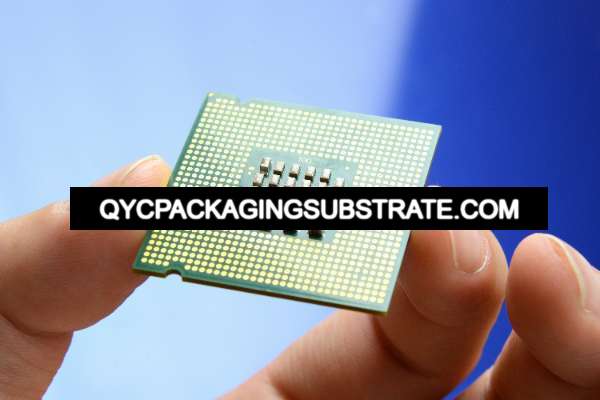
Micro cavity PCB manufacturing
In general, Micro Cavity PCB is a key electronic manufacturing technology that achieves high integration and precise control of electronic devices by integrating electronic components in a tiny space, providing strong support for the development of modern electronic products.
How to design a Micro Cavity PCB?
Designing a Micro Cavity PCB is a delicate and complex process that requires an in-depth understanding of its fundamental principles and steps. The following will introduce in detail how to design Micro Cavity PCB:
Micro Cavity PCB designs are based on traditional printed circuit board technology, but with greater precision in detail and precision. The basic principle is to form tiny concave or convex structures on the surface of the PCB to accommodate specific electronic components or implement specific circuit functions. These microchambers enable higher integration and performance for a variety of high-tech applications.
Requirements analysis: First, the specific requirements and functions of the Micro Cavity PCB need to be clearly designed. This includes determining the number of microchambers required, their size, shape, and their role in the circuit.
Circuit design: Next, circuit design is performed, including the layout of conventional circuits and microchambers. When designing a circuit, it is necessary to consider the connection method and layout optimization between the microcavity and other components to ensure the stability and reliability of the circuit.
Select materials: Choose the appropriate PCB material based on your design needs. For Micro Cavity PCB, special materials with excellent conductivity and insulation properties are usually selected to ensure the manufacturing and use effects of the micro cavity.
CAD design: PCB design using computer-aided design (CAD) software. In CAD software, circuit diagrams and microchamber layouts are drawn, and three-dimensional simulations and optimizations are performed to ensure the accuracy and feasibility of the design.
Routing and Connections: Route and connect individual components and microcavities on the PCB surface according to the circuit design. The wiring process needs to consider the path of signal transmission and the minimization of interference to improve the performance and stability of the circuit.
Verification and optimization: After completing the design, perform verification and optimization. This includes steps such as circuit simulation, prototype testing and performance evaluation to identify and resolve potential issues and optimize the design to meet performance and quality requirements.
Manufacturing file generation: Finally, the files required for manufacturing are generated, including Gerber files and BOM (Bill of Materials) lists, etc. These files will be used for the actual manufacturing and production of the PCB.
Through the above steps, high-quality Micro Cavity PCB design can be achieved to meet the needs of various high-tech applications.
What is the manufacturing process of Micro Cavity PCB?
The manufacturing process of Micro Cavity PCB is a complex and precise process, which involves multiple key steps. Each step is crucial and directly affects the quality and performance of the final product. The manufacturing process of Micro Cavity PCB and its key steps will be introduced in detail below.
First of all, in the manufacturing process of Micro Cavity PCB, the selection of materials is crucial. In general, substrate selection should take into account factors such as required electrical conductivity, mechanical strength, and high temperature resistance. In general, commonly used substrates include FR-4, metal substrates, ceramic substrates, etc.
Secondly, the first step in manufacturing Micro Cavity PCB is coating. This step involves coating a conductive material, usually copper, on the surface of a substrate to create a circuit pattern. This coating usually uses chemical methods to ensure complete bonding of the copper layer to the substrate surface.
Next comes exposure. During the exposure process, the circuit board covered with a photosensitive adhesive layer is passed through a photomask to expose the required circuit pattern. After exposure, the adhesive layer will become soluble due to exposure, thereby forming a circuit pattern pattern.
This is closely followed by etching. In this step, the unexposed photosensitive adhesive layer will be dissolved, exposing the copper layer. The circuit board is then immersed in an etching solution, which etch away the unprotected copper layer, leaving the desired circuit pattern.
Then comes drilling. In this step, a high-precision CNC drilling machine is used to drill holes in the circuit board according to the design requirements. These holes are used to mount components and connect wires between different layers.
Finally, there is electroplating. In this step, metal, such as copper or nickel, is deposited on the surface of the circuit board to enhance conductive properties and protect circuit patterns. Plating can also adjust the electrical characteristics of a circuit board by controlling the thickness of the metal deposited.
In general, the manufacturing process of Micro Cavity PCB includes key steps such as coating, exposure, etching, drilling and electroplating. The precise execution of these steps is crucial to the quality of the final product. Mistakes in any step may lead to circuit board failure or performance degradation. Therefore, every step in the manufacturing process needs to be strictly controlled to ensure product quality and stability.
What are the specific steps for manufacturing Micro Cavity PCB?
Manufacturing Micro Cavity PCBs is a delicate and complex process involving multiple key steps, each of which is vital. Below we will detail the specific steps of Micro Cavity PCB manufacturing.
Before manufacturing Micro Cavity PCB, various materials need to be prepared, including substrate materials, conductive materials, insulating layer materials, etc. The selection and quality of these materials directly affects the performance and quality of the final product.
Next, graphic design and typesetting are performed through CAD software to determine key parameters such as PCB wiring and component locations. This step is an important step in ensuring that the PCB design meets technical requirements and customer needs.
The designed pattern template is placed on the PCB material, and through the process of exposure and etching, the pattern is transferred to the PCB material to form a conductive pattern layer and an insulating layer.
Drill holes in the PCB for mounting electronic components. Electroplating is then performed to increase the thickness of the conductive layer and improve the conductive properties of the PCB.
Paste electronic components on the surface of the PCB and fix them on the PCB through processes such as soldering. In this step, it is necessary to ensure the precise positioning and solid connection of the components.
After assembly, the Micro Cavity PCB is tested and quality controlled. Through electrical testing, functional testing and other means, ensure that the performance and reliability of the PCB meet the requirements.
Finally, the PCB is cleaned to remove surface dirt and residue. It is then packaged to protect the PCB from the external environment, ensuring product integrity and safety.
Through the above steps, a high-quality Micro Cavity PCB completes the manufacturing process. Each step requires strict operation and control to ensure that the final product meets technical standards and customer requirements.
How much does Micro Cavity PCB cost?
Micro Cavity PCB cost is one of the important factors to consider during the manufacturing and design process. Understanding cost structures and estimating methods is critical to project budgeting and decision-making.
The cost of Micro Cavity PCB is affected by many factors, including but not limited to the following aspects:
Layers and Dimensions: The layers and dimensions of a Micro Cavity PCB determine the amount of material required and ease of fabrication, thus directly affecting cost.
Material Selection: PCB material selection has a significant impact on cost. The cost of different materials varies greatly, and some specialty materials may be more expensive.
Line width and spacing: The line width and spacing on Micro Cavity PCB determine the complexity of the manufacturing process, affecting the choice and cost of the production process.
Special processes: If the project requires special processes, such as high-precision micro-machining or special surface treatments, manufacturing costs will increase.
Quantity and batch size: Generally speaking, mass production can lead to lower unit prices because fixed costs can be spread over more products, thus reducing unit costs.
Delivery time: If urgent delivery or expedited manufacturing is required, the manufacturer may need to work overtime or speed up the production schedule, which may increase costs.
Design complexity: The design complexity of Micro Cavity PCB will affect the complexity of the production process and the human resources required, thus directly affecting the cost.
To estimate the cost of a Micro Cavity PCB, you can use the following methods:
Request a Quote: Contact multiple PCB manufacturers to provide design files and request a quote. Compare the quotes from different manufacturers.
Online Cost Calculator: Many PCB manufacturers offer online cost calculators where you can enter your design specifications and requirements and the system will automatically generate an estimated cost.
Cost Analysis Tools: Use professional cost analysis tools to perform detailed cost estimates based on design parameters and material costs.
By comprehensively considering the above factors and using appropriate estimation methods, the cost of Micro Cavity PCB can be estimated relatively accurately, providing a reference for project budgeting and decision-making.
What materials are Micro Cavity PCBs made of?
When manufacturing Micro Cavity PCB, the selection of materials is crucial, because different materials will directly affect the performance, reliability and applicable scenarios of the PCB. Below we will introduce some commonly used Micro Cavity PCB materials and their impact on PCB performance.
FR-4 (Fiberglass Reinforced Epoxy): FR-4 is one of the most common PCB materials and has good electrical properties and mechanical strength making it suitable for most general electronic applications.
FR-4 High Frequency Board: Special FR-4 material designed for high frequency applications, with lower dielectric constant and loss, suitable for circuits requiring higher frequencies and speeds.
Metal substrate: Typically based on aluminum or copper, metal substrates have excellent heat dissipation properties and are suitable for high-power and high-temperature applications such as LED lighting and automotive electronics.
Polyimide (PI): PI material has excellent high temperature resistance and chemical stability, and is suitable for high temperature environments and special industrial applications, such as aerospace and defense fields.
PTFE (polytetrafluoroethylene): PTFE has a low dielectric constant and loss, as well as excellent chemical resistance, making it suitable for microwave and radio frequency applications such as communications and radar systems.
Impact of Material Selection on Micro Cavity PCB Performance
Electrical performance: Different PCB materials have different dielectric constants and losses. Choosing the appropriate material can ensure the stability and accuracy of the circuit’s signal transmission.
Mechanical Strength: The mechanical strength of the PCB material directly affects the durability and reliability of the PCB, especially in applications where it may be subject to vibration and shock.
Thermal management: Metal substrates have excellent heat dissipation properties and can effectively conduct heat to the environment, thereby reducing the operating temperature of electronic components and improving system performance and life.
Environmental adaptability: For applications that need to work in harsh environments, such as high temperature, high humidity or chemically corrosive environments, it is crucial to choose materials that are resistant to high temperatures and corrosion.
Manufacturing costs: The costs of different materials vary greatly, and a balance between material performance and cost needs to be considered to meet project budgets and requirements.
In summary, the correct choice of materials for Micro Cavity PCB is critical to ensuring circuit performance and reliability. Depending on the application requirements and budget constraints, the rational selection of suitable materials will lay a solid foundation for the successful implementation of the project.
Who makes Micro Cavity PCBs?
In the world of Micro Cavity PCB manufacturing, supplier selection is crucial. In our company, we are not only your supplier, but also your partner. We are committed to providing our customers with the highest quality Micro Cavity PCB solutions to meet their high performance and precision needs.
Professional experience: Our company has many years of Micro Cavity PCB manufacturing experience. Our team has deep technical accumulation and rich industry experience, and can provide customers with professional consulting and technical support.
Advanced Equipment: We use the most advanced equipment and technology for production to ensure that the quality and precision of Micro Cavity PCB meet customer requirements.
Strict quality control: Our company strictly follows the ISO quality management system and conducts strict quality control in every aspect from raw material procurement to production and manufacturing to ensure that products meet customer standards.
Customized services: We provide customized solutions, tailoring the most suitable Micro Cavity PCB according to customers’ needs and application scenarios to meet their specific needs and requirements.
Stable supply chain: The company has established long-term and stable cooperative relationships with reliable suppliers to ensure a stable supply of raw materials and continuity of production, thereby providing customers with a stable supply of products.
Timely response: We focus on communication and communication with customers, respond to customer needs and problems in a timely manner, and ensure that customers can receive satisfactory solutions in a timely manner.
When it comes to choosing a Micro Cavity PCB manufacturer, you’ll make the right choice by choosing our company. We will wholeheartedly provide you with high-quality products and professional services, and create a future with you!
What are the five characteristics of great customer service?
High-quality customer service refers to the high-level, personalized service experience that companies provide customers and meet their needs. It goes beyond a simple transactional process and is built on positive interaction, effective communication and ongoing relationships. Quality customer service not only meets customers’ needs and expectations, but exceeds them, building long-term trust and loyalty.
Timely response: Responding promptly and providing solutions when customers raise questions or needs is a basic requirement for quality customer service. Quick response can make customers feel valued and enhance their trust and satisfaction.
Professional knowledge: Having professional knowledge and skills is an important prerequisite for providing excellent customer service. Employees should understand the company’s products or services and be able to provide accurate and clear answers to customers’ questions, as well as provide professional advice and guidance.
Customized solutions: Great customer service should be personalized and provide customized solutions based on the customer’s needs and circumstances. Understand customers’ preferences and requirements and flexibly adjust service content to meet their individual needs.
Good communication: Effective communication is the basis for building a good customer relationship. Employees should be good at listening to customers’ opinions and feedback, communicate and solve problems in a timely manner, and ensure that information is transmitted accurately and clearly.
After-sales support: Providing comprehensive after-sales support is an important part of excellent customer service. Enterprises should provide customers with after-sales service and support, including product maintenance, return and exchange policies, technical support, etc., to ensure customer satisfaction and confidence in the use of products or services.
To sum up, high-quality customer service is not only an interactive process between enterprises and customers, but also an important means to establish long-term relationships and enhance brand value. Through key features such as timely response, expertise, customized solutions, good communication and after-sales support, companies can enhance customer experience and win their trust and loyalty, thereby achieving sustained growth and success.
FAQS
What are the typical applications of Micro Cavity PCBs?
Micro Cavity PCBs find applications in various high-tech industries such as telecommunications, medical devices, aerospace, automotive electronics, and consumer electronics. They are particularly useful in devices requiring high precision and compact design.
What are the advantages of using Micro Cavity PCBs?
Micro Cavity PCBs offer several advantages, including reduced size and weight of electronic devices, improved thermal management, enhanced signal integrity, and increased reliability. Additionally, they allow for the integration of complex circuitry in a smaller footprint.
What factors influence the cost of Micro Cavity PCBs?
The cost of Micro Cavity PCBs depends on factors such as the complexity of the design, the choice of materials, the manufacturing process used, and the volume of production. High-density designs with intricate features may incur higher costs compared to standard PCBs.
What materials are commonly used in Micro Cavity PCB manufacturing?
Materials commonly used in Micro Cavity PCB manufacturing include FR-4, high-frequency laminates such as Rogers, polyimide, and ceramic substrates. The choice of material depends on the specific application requirements, such as impedance control, thermal conductivity, and flexibility.
How do you ensure the reliability of Micro Cavity PCBs?
Reliability of Micro Cavity PCBs is ensured through rigorous testing and quality control measures throughout the manufacturing process. This includes design verification, material inspection, process control, and testing of finished PCBs for functionality and performance.