 Professional Flip-Chip Packaging Substrate Supplier

Micro PCB Substrate Manufacturer, we mainly produce ultra-small bump pitch substrate, ultra-small trace and spacing packaging substrate and PCBs.
In today’s technology field, micro PCB substrates have become an indispensable and important part of the design and manufacturing of electronic equipment. From smartphones to medical devices, micro PCB substrates play a key role. This article will delve into the definition, design principles, and manufacturing processes of micro PCB substrates, aiming to provide readers with an in-depth understanding of this field.
What is Micro PCB Substrate?
Micro PCB substrate is a key component for the layout and connection of electronic components in a very small size range. Compared with traditional printed circuit boards (PCBs), micro PCB substrates are more outstanding in size and density, so they perform well in applications that require compactness and high performance. The design and manufacturing of these micro-substrates requires a high degree of precision and technology to meet the miniaturization and high performance demands of modern electronic devices.
As electronic products become increasingly miniaturized, micro PCB substrates have become an important tool to achieve this goal. They can accommodate multiple electronic components in an extremely limited space and combine them efficiently through sophisticated connections. This high-density layout enables micro PCB substrates to meet the compact design needs of small electronic products such as smartphones and wearable devices, while also providing excellent performance and reliability.
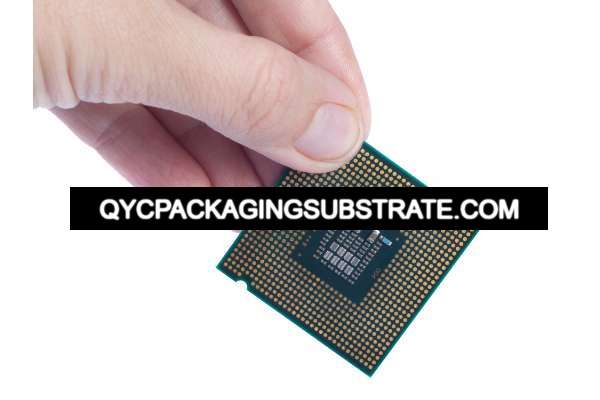
Micro PCB Substrate Manufacturer
In addition to applications in consumer electronics, micro PCB substrates are also widely used in medical equipment, industrial control systems, aerospace and other fields. In these areas, the requirements for high performance and reliability are more stringent, and micro PCB substrates are ideally suited to meet these needs.
Overall, micro PCB substrates play an integral role in modern electronics. They not only promote the development of miniaturization and high performance of electronic products, but also provide powerful support and solutions for various application scenarios. With the continuous advancement and innovation of technology, I believe that micro PCB substrates will continue to play an important role in the future and bring more surprises and breakthroughs to the electronics industry.
Micro PCB Substrate design Reference Guide.
When designing a micro PCB substrate, designers must consider several key factors to ensure its performance and stability. Here are some design reference guides to help you better plan and implement your micro PCB substrate design:
Space utilization
In micro PCB substrate design, space is a critical resource. Designers need to make full use of every square millimeter of space to accommodate as many electronic components and connections as possible. Adopting a compact layout design can minimize the substrate size and improve the overall performance and portability of the device.
Thermal management
Because micro PCB substrates typically have high levels of integration and power density, thermal management is an important consideration. Designers should properly plan heat dissipation structures, such as heat sinks and heat dissipation holes, to effectively remove heat and keep components operating within a safe temperature range.
Signal integrity
In micro PCB design, signal integrity is critical, especially in high-speed digital and analog circuits. Designers need to pay attention to the length, wiring method and impedance matching of signal lines to ensure the stability and reliability of signal transmission. The use of differential signal transmission and noise suppression technology can effectively improve the anti-interference ability of the signal.
Material selection
Choosing the right materials is critical to the performance and reliability of your micro PCB substrate. Commonly used materials include polyimide (PI), polytetrafluoroethylene (PTFE), and metallized ceramics, which have excellent mechanical properties, high temperature resistance, and electrical properties. Designers should select the most appropriate material based on specific application needs and environmental conditions.
High Density Interconnect Technology
To achieve higher integration and performance density, designers can use high-density interconnect technologies such as micro-lines, blind vias, and buried vias. These technologies can effectively reduce the spacing between components, improve the flexibility and density of circuit layout, and reduce the delay and loss of signal transmission.
The design of micro PCB substrate is a complex and critical process. Designers need to comprehensively consider multiple factors such as space utilization, thermal management, signal integrity, etc. Through precise layout planning, appropriate material selection and the application of high-density interconnection technology, micro PCB substrates can be ensured to have stable performance and reliable operation.
What material is used in Micro PCB Substrate?
The material of the micro PCB substrate is very important, which directly affects its performance, stability and scope of application. Typically, in order to meet high performance and special needs, micro PCB substrates use a range of high performance materials. Several commonly used materials will be introduced in detail below:
Polyimide (PI) is a high-temperature material with excellent electrical properties and chemical stability. Due to its excellent high temperature resistance, PI is often used in the manufacture of micro PCB substrates, allowing it to maintain stability in extreme working environments. In addition, PI materials also have good mechanical strength and solvent resistance, making them suitable for use in high-performance electronic equipment.
Another commonly used material is polytetrafluoroethylene (PTFE), a material with excellent insulating properties and high temperature resistance. The application of PTFE in micro PCB substrates gives it excellent high-frequency characteristics and is suitable for applications requiring high-speed signal transmission. In addition, PTFE also has excellent chemical stability and corrosion resistance, allowing it to maintain stability in harsh environments.
In addition to the common materials mentioned above, metallized ceramic substrates are also widely used in some special application scenarios. Metallized ceramic substrates combine the properties of metal and ceramics, have excellent thermal conductivity and mechanical strength, and are suitable for high-power and high-frequency electronic equipment.
Overall, micro PCB substrate material selection depends on specific application needs and performance requirements. Designers need to choose appropriate materials based on the actual situation to ensure that the micro PCB substrate can work stably and reliably in various working environments.
What size are Micro PCB Substrate?
Micro PCB substrates play an important role in modern electronic devices, and their dimensional accuracy and adaptability are critical to the device’s performance and functionality. Since micro PCB substrates are typically used in small devices, their dimensions are relatively small, but while remaining compact, they must meet the requirements of the specific application.
The size of a micro PCB substrate may be only a few millimeters to tens of millimeters. In modern electronics, size is critical to the design and manufacturing process. For example, in small devices such as smart watches, headphones, and medical equipment, the size of the micro PCB substrate must be small enough to fit into limited space and still maintain high performance and reliability.
However, size is not the only consideration. The size of the micro PCB substrate must be coordinated with other factors, such as circuit layout complexity, electrical performance needs, and thermal management requirements. Therefore, when designing micro PCB substrates, engineers must weigh these factors to ensure that the final product can provide excellent performance within the restricted space.
Another factor to consider is advances in manufacturing technology. As manufacturing technology continues to develop, the size range of micro PCB substrates is also expanding. Modern manufacturing technologies make it possible to achieve more complex circuit layouts and higher levels of integration in tiny sizes, providing more possibilities for a variety of applications.
In general, micro PCB substrates come in a wide range of sizes, ranging from a few millimeters to tens of millimeters. When designing and manufacturing micro PCB substrates, engineers must consider the requirements of specific applications and take full advantage of modern manufacturing technologies to achieve optimal performance and reliability.
The Manufacturer Process of Micro PCB Substrate.
The manufacturing process of micro PCB substrates is a highly precise process involving multiple critical steps to ensure the quality and reliability of the final product. These steps are detailed below:
Graphic Design
The first step in manufacturing a micro PCB substrate is graphic design. Designers use professional PCB design software to draw circuit diagrams according to product requirements and specifications, and determine the layout and connection of components. Precision and accuracy are crucial at this stage, as the quality of the design directly affects the performance and reliability of the final product.
Lithography
After the graphic design is completed, the circuit diagram will be transferred to the PCB substrate using photolithography technology. In this step, a layer of light-sensitive photoresist is coated on the surface of the substrate, and the designed circuit diagram is projected onto the photoresist through a photolithography machine. The unexposed photoresist is then chemically removed, leaving the desired circuit pattern.
Etching
After photolithography is completed, the etching step follows. At this stage, a chemical solution is used to etch away the metal layer not covered with photoresist from the PCB substrate, creating a circuit pattern. This process requires highly precise control to ensure the accuracy and clarity of circuit patterns.
Metalization
After etching is completed, the PCB substrate needs to be metallized. This means applying a layer of metal (usually copper) over the circuit pattern to create circuit connections and conductivity. Metalization can be achieved through chemical methods or techniques such as vacuum evaporation to ensure the stability and conductivity of the connection.
Throughout the manufacturing process, manufacturers need to strictly control each step to ensure the quality and reliability of micro PCB substrates. Errors or poor handling in any link may lead to substandard final products. Therefore, precise process control and high-quality equipment and materials are the keys to manufacturing micro PCB substrates.
The Application area of Micro PCB Substrate.
Micro PCB substrates play an irreplaceable role in the field of modern technology, and their wide range of applications cover multiple industries, from consumer electronics to medical equipment to aerospace. These small size, high performance substrates are ideal for many modern devices. Here are some common application areas:
Consumer Electronics
Micro PCB substrates play a vital role in consumer electronics. For example, portable devices such as smartphones, tablets, and smart watches require compact and efficient circuit boards to implement various functions. The small size and high performance of micro PCB substrates allow these devices to implement complex functions in limited space while maintaining good performance and reliability.
Medical equipment
In the medical industry, micro PCB substrates are widely used in various medical devices, including pacemakers, medical monitoring instruments, medical imaging equipment, etc. These devices often require highly reliable circuit boards to ensure accurate data collection and stable operation. The high performance and stability of micro PCB substrates make them the first choice for medical device manufacturers.
Aerospace
In the aerospace field, the demand for micro PCB substrates is also growing. Aerospace equipment has very strict requirements for electronic components. They must be able to work normally under extreme environmental conditions and have a high degree of anti-interference ability. The small size and high performance of micro PCB substrates make them ideal for aerospace electronic systems, meeting complex operating requirements and delivering superior performance.
Other areas
In addition to the above fields, micro PCB substrates are also widely used in many other industries, including automobile manufacturing, industrial automation, communication equipment, etc. Whether it is an electronic control unit in a car central control system or a control panel in a factory automation system, micro PCB substrates play an important role in promoting technological innovation and development in all walks of life.
In summary, micro PCB substrates have a wide range of applications, and their small size, high performance, and reliability make them an indispensable part of many modern devices. With the continuous advancement of technology and the growing demand for applications, micro PCB substrates will continue to play an important role and play an increasingly important role in various industries.
What are the advantages of Micro PCB Substrate?
When it comes to the advantages of micro PCB substrates, they have several significant advantages over traditional PCBs. Here’s a more detailed look at these benefits:
Higher integration
Micro PCB substrates enable more functions and component integration in limited space. By using advanced manufacturing technology and compact design, micro PCBs can integrate a large number of electronic components onto a small substrate to achieve highly integrated circuits. This increase in integration makes micro PCBs more widely used in small devices and products, bringing greater flexibility to the design of electronic products.
Smaller size
Compared with traditional PCB, micro PCB substrate has smaller size. This makes them particularly suitable for applications with strict space requirements, such as portable electronic devices, medical equipment and smart wearable devices. The small size of the micro PCB makes the entire device lighter and more portable, and can implement complex functions in a more restricted space.
Higher performance density
Micro PCB substrates can achieve more functions and connections per unit area. By using high-density interconnection technology and miniaturized components, micro PCBs can achieve higher performance density, allowing components on the circuit board to be laid out more closely. This high-performance density not only improves board functionality but also reduces board size and weight, further enhancing overall product performance.
Excellent electrical performance and reliability
Micro PCB substrates typically use high-performance materials and advanced manufacturing processes to ensure they provide excellent electrical performance and reliability under a variety of operating conditions. This reliability has led to the widespread use of micro PCBs in critical applications such as medical equipment and aerospace. At the same time, micro PCBs can also provide better thermal management and anti-interference performance, ensuring that electronic products can operate stably in various environments.
To sum up, micro PCB substrates have higher integration, smaller size and higher performance density than traditional PCBs, while also providing excellent electrical performance and reliability. These advantages make micro PCBs play an increasingly important role in the design and manufacturing of modern electronic equipment, providing more flexible and reliable solutions for various application scenarios.
FAQ
What is the minimum size of a micro PCB substrate?
The size of the micro PCB substrate can vary depending on the application. Typically, the size of micro PCB substrates can be reduced to the range of a few millimeters. However, determining the minimum size depends on the required circuit layout and component sizes, as well as manufacturing process constraints.
How much does it cost to manufacture a micro PCB substrate?
The manufacturing cost of micro PCB substrates is affected by several factors, including the cost of the materials selected, design complexity, manufacturing process complexity, and production scale. Typically, as size decreases and technology improves, manufacturing costs may increase. However, mass production often reduces the cost per unit.
What is the operating temperature range that a micro PCB substrate can withstand?
The operating temperature range of the micro PCB substrate depends on the performance characteristics and design requirements of the selected material. Generally speaking, micro PCB substrates can usually operate over a wide temperature range, such as -40°C to +125°C. However, in some special application scenarios, it may be necessary to choose materials that are more resistant to high or low temperatures to meet specific working environment requirements.
How difficult is it to solder a micro PCB substrate?
Since micro PCB substrates are typically higher density and smaller in size, soldering can be more challenging. For tiny solder joints and tight arrangements, high-precision soldering techniques such as surface mount technology (SMT) and reflow soldering are required. In addition, due to the limited heat dissipation capacity of the micro PCB substrate, special attention needs to be paid to temperature control during the welding process to prevent damage to sensitive components or welding defects.
What are the special considerations for using micro PCB substrates in medical devices?
When using micro PCB substrates in medical devices, special considerations need to be given to biocompatibility, reliability and stability. Since medical devices are often in direct contact with the human body, the material selection and manufacturing process of micro PCB substrates must comply with strict medical standards and regulations. In addition, medical equipment has extremely high reliability requirements, so the design and manufacturing of micro PCB substrates must undergo rigorous verification and testing to ensure its reliability and safety under various working conditions.