 Professional Flip-Chip Packaging Substrate Supplier

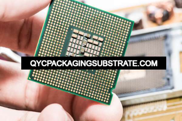
Microtrace PCB manufacturing. High speed and high frequency material bga packaging substrate, led pcb, hdi pcb manufacturing. Advanced Microtrace production technology.
What is a Microtrace PCB?
Microtrace PCB is a highly complex circuit board commonly used to implement high-density and high-performance electronic functions in miniature electronic devices. They play a vital role in modern technology, especially in fields such as computers, communication equipment, medical equipment, and consumer electronics.
Microtrace PCBs typically use micro-manufacturing processes where the components and wires on the board are often smaller than part of a traditional circuit board. This small size allows Microtrace PCBs to achieve higher component density, enabling more functionality in a limited space. In addition, Microtrace PCBs are able to offer higher performance and lower circuit noise, making them ideal for many high-end applications.
The manufacturing of Microtrace PCBs often involves advanced processes, including techniques such as laser cutting, chemical etching, and micro-soldering. These technologies ensure the accuracy and stability of the circuit board to ensure its reliability and durability under various environmental conditions.
In general, Microtrace PCB represents one of the latest advances in the field of electronic engineering. Their emergence makes it possible to realize complex electronic functions in a limited space, providing important support for the development of modern technology.
Microtrace PCB manufacturing
How to Design a Microtrace PCB?
Designing a micro-tracking PCB requires certain expertise and skills, here is a brief guide:
Determine the requirements and specifications: Before designing the PCB, you must first clarify the requirements and specifications. This includes determining the circuit’s functionality, performance specifications, size requirements, etc.
Choose the right software: Choose a professional software suitable for designing micro-tracking PCB, such as Altium Designer, Cadence Allegro, etc. These software provide a wealth of features and tools to meet the needs of micro-tracking PCB design.
Draw schematic diagram: Use design software to draw the schematic diagram of the circuit based on requirements and specifications. When drawing the schematic diagram, factors such as the functional partitioning of the circuit and the signal transmission path should be considered.
Layout design: Design the layout of the PCB according to the schematic diagram. The goal of layout design is to minimize the electromagnetic interference of the circuit and ensure the stability and reliability of signal transmission. In layout design, attention needs to be paid to minimizing stray capacitance, inductance and other components on the circuit board, as well as reducing the length of the signal transmission path.
Trace design: According to the layout design, conduct trace design on the PCB. The wiring design must consider factors such as signal transmission speed and impedance matching to ensure the stability and reliability of signal transmission. In the trace design, the width and spacing of the traces should be minimized to reduce the size of the micro-tracking PCB.
Consider ground and power: In PCB design, the design of ground and power is crucial. The design of the ground wire and power supply should consider reducing the ground potential difference and voltage fluctuation of the circuit to ensure stable operation of the circuit.
Conduct simulation and verification: After the PCB design is completed, conduct simulation and verification. Use simulation software to simulate the PCB to verify the performance and stability of the circuit. If necessary, prototype verification can be performed to further verify the performance and reliability of the PCB.
Manufacturing and Assembly: After the PCB design is completed, it is submitted to the PCB manufacturing factory for manufacturing. After manufacturing is completed, the PCB is assembled and tested. During the assembly and testing process, attention should be paid to checking the quality and performance of the PCB to ensure that it meets the design requirements.
Designing micro-tracking PCB requires comprehensive consideration of circuit design, layout design, wiring design and other factors. Only by comprehensively considering these factors can we design a micro-tracking PCB with stable performance and high reliability.
What is the Microtrace PCB Fabrication Process?
The microtrace PCB manufacturing process is an advanced process for producing printed circuit boards (PCBs) that is carefully designed and optimized to ensure high quality and reliability. The process consists of multiple steps, with a detailed flow from designing prototypes to the production of the final product.
First, the design phase is key to the entire process. Design engineers use CAD software to create prototypes of PCBs, including layout, routing, arrangement of connectors, and other components. At this stage, special attention is paid to ensuring the performance and reliability of the circuit board.
Next is prototyping the circuit board. Through photolithography, the designed pattern is transferred to a photosensitive layer covering the copper foil. Chemical etching is then used to etch away the portions of the copper that were not protected by the photolithography, creating the circuit board’s conductors. This step is very critical as it determines the accuracy and quality of the circuit board.
Then stack the multi-layer circuit boards. In this step, multiple single-layer PCBs are pressed together to form a multi-layer structure. Each layer has its own copper foil and insulation layer, with via hole punching technology connecting the wires between the different layers.
Next comes surface treatment. The surface of the circuit board usually needs to be coated with a layer of protective metal, such as gold plating or tin plating, to improve its corrosion resistance and soldering performance.
Finally comes quality control and testing. After production is complete, each circuit board goes through rigorous quality control and testing procedures to ensure it meets specifications and works reliably. This may involve visual inspection, electrical testing, and environmental endurance testing.
Overall, the microtrace PCB manufacturing process is a complex and delicate process involving multiple steps and technologies. Through strict design, manufacturing and testing procedures, it ensures the production of high-quality, reliable printed circuit boards that meet the needs of various applications.
How to manufacturing a Microtrace PCB ?
Micro-tracking PCB manufacturing involves multiple steps, requiring meticulous planning and operation from design to production. Here are the rough steps:
Design and planning: First, determine the design requirements and specifications of the PCB. This may include determining board size, number of layers, routing rules, etc. Designers use professional PCB design software to create schematics and layouts.
Manufacturing raw material preparation: Determine required substrate materials and coatings. Commonly used substrate materials include FR-4 fiberglass composites. Coatings may include copper foil, etc.
Graphic visualization: Use CAD software to convert designs into machine-readable file formats. These files include information such as PCB layers, wiring, and hole locations.
Pre-production preparation: Prepare production equipment, including CNC drilling machines, etching machines and automatic assembly equipment. Check that all equipment is working properly.
Printed circuit board: Using photolithography technology to transfer the designed pattern onto the substrate. This involves applying a photosensitive paint and then using a photomask to project a pattern onto the coating. After exposure, the paint is removed from the unexposed areas through chemical treatment.
Electroplating: Electroplating a thin layer of copper on a printed circuit board to increase electrical conductivity. The commonly used method is to perform electroplating on the exposed copper foil surface to fill holes and increase the thickness of the circuit.
Chemical Etching: Using a chemical etchant, such as iron chloride, to remove unprotected copper to create the desired circuit pattern.
Stripping the photosensitive coating: The photosensitive coating is removed from the printed circuit board to reveal the final pattern of the board.
Pads and Assembly: Add pads to the PCB, which are used to connect components. The components are then soldered to the PCB using automated equipment.
Testing and Quality Control: Finished PCBs are tested to ensure they meet specifications and are free of defects. This may involve the use of test fixtures and automated test equipment.
Packaging and delivery: The completed PCB will be packed and delivered to the customer according to the order requirements.
The above are the general steps for micro-tracking PCB manufacturing, but the actual manufacturing process may vary depending on the manufacturer and specific needs.
How Much Does a Microtrace PCB Cost?
The cost of microtracking PCBs depends on a variety of factors, including but not limited to board material, laminate construction, size, design complexity, and production volume. Typically, the cost of micro-tracking PCBs may be higher than regular PCBs because micro-tracking PCBs require higher precision and technical requirements.
For a basic microtrace PCB, the cost can range from tens to hundreds of dollars. However, for more complex designs such as multi-layer PCBs, high-frequency circuits or embedded components, the cost can increase significantly. In addition, production volume will also have an impact on costs. Typically, costs decrease as production volume increases.
Overall, if you need to obtain an accurate micro-tracking PCB cost estimate, it is best to provide the PCB manufacturer with detailed design specifications and requirements so that they can provide an accurate quote.
What materials are Microtrace PCB made of?
Microtracking (PCB) is mainly composed of several materials, which play a key role in the manufacturing process of PCB. The following are common Microtrace PCB materials:
Substrate material: Microtrace PCB usually uses glass fiber reinforced epoxy resin as the substrate material. This substrate material has good electrical properties and mechanical strength and is suitable for PCB manufacturing and long-term use.
Conductive layer material: The conductive layer of Microtrace PCB is usually composed of copper. Copper is an excellent conductive material that provides good electron transport properties and is relatively easy to process into the desired shape.
Insulating layer material: The insulating layer of Microtrace PCB is usually made of materials such as epoxy resin or polytetrafluoroethylene (PTFE). These materials have good insulation properties and can effectively prevent unnecessary leakage or interference of current on the PCB.
Soldering Material: The soldering material used to connect electronic components in Microtrace PCB is usually solder or solder. These materials are able to melt at high temperatures and form reliable connections, ensuring a good connection between electronic components and PCBs.
Impedance Control Materials: For some Microtrace PCB applications, precise control of the signal’s impedance is required. In this case, the PCB manufacturer may use special materials, such as fiberglass composites containing specific dielectric constants, to ensure the required impedance matching.
To sum up, Microtrace PCB usually consists of glass fiber reinforced epoxy resin substrate, copper conductive layer, insulating layer material, soldering material and possible impedance control material. The selection and use of these materials ensures that Microtrace PCB has good electrical properties, mechanical properties and reliability.
Who manufactures Microtrace PCB ?
Microtrace PCB is a high-performance printed circuit board (PCB) with sophisticated tracking and monitoring capabilities. It is manufactured by the company’s professional team using the most advanced technology and craftsmanship. Microtrace PCB not only has excellent electrical performance, but also has high reliability and stability, and is suitable for various complex electronic equipment and systems.
The manufacturing process of Microtrace PCB begins with carefully selected high-quality substrates. We use advanced material selection techniques to ensure every component meets strict quality standards. Next, through precise chemical treatment and mechanical processing, the surface of the substrate is smoothed and the ideal roughness and flatness are ensured, laying a solid foundation for subsequent process steps.
During the wiring stage, we use state-of-the-art CAD/CAM technology to translate the circuit design into an actual physical layout. Through precise control and optimization, the circuit layout of Microtrace PCB is optimized to the greatest extent to ensure the best performance and stability of signal transmission. Our team of engineers work closely together to rigorously review and optimize the layout to ensure every component is optimally positioned and connected on the PCB.
In the printing stage, we use advanced printing technology to print circuit patterns on the substrate. We use high-precision printing equipment and selected printing materials to ensure the clarity and accuracy of the pattern. Each process undergoes strict quality control to ensure that the printing results meet the design requirements and have a high degree of reliability and stability.
During the component installation and welding stages, we use advanced automated equipment and precise processes to accurately install the components on the PCB and achieve reliable connections through high-temperature welding technology. Our process flow has been optimized and improved many times to ensure the efficiency and stability of component installation, providing a solid guarantee for the performance and reliability of the final product.
Finally, during the testing and verification phase, we use strict testing standards and advanced testing equipment to conduct comprehensive functional testing and performance verification on each Microtrace PCB. Our testing process covers a variety of working and environmental conditions to ensure that the product will work properly and perform optimally under all circumstances.
Overall, Microtrace PCB is a high-performance, reliable and stable printed circuit board with sophisticated tracking and monitoring capabilities. It is manufactured by the company’s professional team using the most advanced technology and processes. It is suitable for various complex electronic equipment and systems, providing customers with excellent quality and reliability guarantee.
What are 5 qualities of a good customer service?
Excellent customer service has many qualities, but five key qualities include:
Responsive: A good customer service team should be able to respond promptly to customer needs and questions. They should respond quickly to phone calls, emails, or online chats and take immediate action when customers raise questions or complaints. Timely responses enhance customer satisfaction, demonstrate professionalism, and build good customer relationships.
Expertise: A good customer service representative should have in-depth knowledge of the product or service they offer. They should be able to accurately answer customer questions, provide detailed solutions, and provide relevant advice or guidance to customers when needed. Expertise not only helps solve customer problems, but also enhances customer trust and loyalty to the brand.
Patience and Friendliness: A good customer service representative should demonstrate patience and friendliness, no matter how complex or finicky the customer’s question is. They should listen to their customers’ needs and opinions, respect their feelings, and communicate with them in a polite and kind manner. A patient and friendly attitude can help ease tensions, facilitate effective communication, and ultimately resolve problems.
Problem-solving skills: A good customer service representative should have the ability to solve problems, regardless of their complexity. They should be able to identify and analyze customer problems, find creative solutions, and solve problems in the shortest possible time. Problem-solving skills can increase customer satisfaction, reduce customer retention, and earn a good reputation for your brand.
Continuous improvement: A good customer service team should constantly seek to improve and improve their service levels. They should regularly collect customer feedback, analyze customer experience, and make adjustments and improvements based on feedback. Continuous improvement can help customer service teams keep up with market changes and changes in customer needs, improve service quality, and maintain a competitive advantage.
FAQS
What is Microtrace PCB?
Microtrace PCB is a company specializing in the design, manufacturing and assembly of printed circuit boards. We provide customized PCB solutions to meet various customer needs.
What services does Microtrace PCB provide?
We provide printed circuit board design, manufacturing and assembly services. Whether it’s a single-layer, double-layer or multi-layer PCB, we can meet our customers’ needs. In addition, we also provide services such as rapid prototyping and mass production.
What are the advantages of Microtrace PCB?
We have advanced manufacturing equipment and technical teams to provide customers with high-quality, high-reliability PCB products. We focus on quality control and customer service and are committed to providing customers with satisfactory solutions.
What does Microtrace PCB’s product range include?
Our product range covers various types of printed circuit boards, including conventional FR-4 PCB, aluminum-based PCB, flexible PCB, etc. We can also customize PCBs with special materials and special processes according to customer requirements.