 Professional Flip-Chip Packaging Substrate Supplier

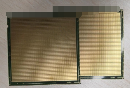
Microtrace RF PCB Manufacturer, and RF package substrates production , we mainly produce ultra-small bump pitch RF BGA substrate, ultra-small trace and spacing BGA packaging substrate from 4 layer to 22 layers.
In today’s wireless communication field, the status of RF (radio frequency) PCB cannot be underestimated. They are not only the key components to support radio frequency electronic components, but also the key to ensuring the stability and performance of communication equipment. This article will give you an in-depth understanding of the RF PCB manufacturing process, and focus on Microtrace, a leading RF PCB manufacturer, to show how they provide customers with excellent solutions.
What is RF PCB?
RF PCB, the full name of Radio Frequency Printed Circuit Board, is a printed circuit board specially designed to process radio frequency signals. Compared with traditional circuit boards, RF PCBs have more precise design and manufacturing requirements to ensure stable performance and reliability at high frequencies. This specialized design makes RF PCB widely used in wireless communications, radar systems, satellite communications and other fields.
The special structure and materials of RF PCB are its key points. In terms of design, RF PCB usually uses structures such as microstrip lines, symmetrical distribution, ground planes, and high-frequency transmission lines to minimize signal loss and interference. At the same time, RF PCB uses special materials, such as PTFE (polytetrafluoroethylene) and FR-4, which have low dielectric constant and loss factor and can maintain stable signal transmission performance at high frequencies.
Microtrace, as a leading company specializing in RF PCB manufacturing, is committed to providing customers with high-performance solutions. We have advanced production equipment and technical teams to meet customers’ various needs in the fields of wireless communications, radio frequency transmission and antenna systems. Whether it is for radio frequency applications with strict frequency requirements or for high-density layout of wireless communication equipment, Microtrace can provide customized RF PCB solutions to ensure that customer projects can be successfully implemented and achieve expected performance indicators.
Overall, RF PCBs play a vital role in modern wireless communications, and their design and manufacturing require a high degree of expertise and technology. As an RF PCB manufacturer, Microtrace will continue to adhere to high-quality, high-reliability manufacturing standards and provide customers with the best products and services.
Microtrace RF PCB
How to design RF PCB?
The design of RF (radio frequency) PCB is a complex and critical process that requires consideration of many factors to ensure that the final product can provide stable performance and reliability at high frequencies. Microtrace’s engineering team relies on its rich experience and expertise to provide customers with customized RF PCB design services to meet their specific application needs.
First, the RF PCB must be designed with the operating frequency in mind. Different frequencies require different PCB layout and characteristics. For example, high-frequency signals require shorter transmission lines and smaller board sizes to reduce signal transmission delays and losses.
Secondly, transmission line characteristics are one of the important considerations in RF PCB design. Factors such as impedance matching, length matching, and interlayer coupling of transmission lines will affect the signal transmission quality. Microtrace’s engineering team utilizes advanced simulation tools and techniques to precisely design and analyze transmission lines to ensure excellent signal transmission performance at high frequencies.
In addition, noise and interference are also issues that need to be paid attention to in RF PCB design. RF signals are very sensitive to noise and interference, so a series of measures need to be taken during the design process to reduce noise levels and suppress external interference. Microtrace’s engineering team has extensive experience in PCB layout, ground design, shielding and filtering, and can effectively manage and control noise and interference to ensure the stability and reliability of RF PCB.
Finally, Microtrace’s engineering team will tailor-make RF PCB design solutions based on customers’ specific needs and application scenarios. Whether in communications, radar, wireless sensors or other fields, we can provide high-performance, high-reliability RF PCB solutions that meet customer needs.
In short, the design of RF PCB needs to comprehensively consider multiple factors such as frequency, transmission line characteristics, noise and interference. Microtrace’s engineering team relies on its professional knowledge and experience to provide customers with customized design services to ensure that RF PCBs can achieve optimal performance and reliability in various application scenarios.
What is the manufacturing process of RF PCB?
The manufacturing process of RF PCB is a delicate and complex process that requires multiple key steps. Each step is crucial and directly affects the performance and quality of the final product. The following will introduce in detail the manufacturing process of RF PCB and how Microtrace ensures that each RF PCB has excellent performance and reliability.
Raw material preparation: The manufacturing process of RF PCB starts with the preparation of raw materials. In Microtrace’s factory, we use high-quality base materials, such as PTFE (polytetrafluoroethylene), FR-4, etc. These materials have excellent insulation properties and high temperature resistance and can meet the requirements of high-frequency signal transmission.
Sheet Processing: Next comes the sheet processing stage, where the raw material is cut into substrates of the required size. Microtrace has advanced processing equipment and technology to accurately process RF PCB substrates that meet design requirements.
Printing: In the printing stage, the circuit pattern and component layout are printed on the substrate according to the design drawings. This step requires precision printing equipment and high-quality printing materials to ensure that the printed circuit patterns are accurate.
Molding: Molding is the process of curing and hot pressing the printed circuit board to form a stable structure. Microtrace uses advanced molding technology to ensure each RF PCB has a solid structure and good dimensional stability.
Assembly: The last is the assembly stage, where various electronic components, such as chips, resistors, capacitors, etc., are welded to the RF PCB according to the design requirements. Microtrace’s team of engineers has extensive assembly experience and can ensure the accuracy and reliability of the assembly process.
Microtrace adopts a strict quality control process. From raw material procurement to final product delivery, every process undergoes rigorous inspection and testing to ensure that each RF PCB has excellent performance and reliability. We are committed to providing customers with high-quality, high-reliability RF PCB solutions to meet their specific application needs.
How much does it cost to manufacture an RF PCB?
RF PCB manufacturing costs are a critical factor in any project, and these costs are affected by a variety of factors. First, considering the type of board the PCB is made of, choosing the right material is critical to achieving the desired performance. For RF PCB, common materials include PTFE (polytetrafluoroethylene) and FR-4. Their price and performance vary greatly, so choosing the appropriate plate type has an important impact on the cost.
Secondly, the number of layers is also one of the important factors affecting RF PCB manufacturing costs. The number of layers refers to the number of stacks of PCB boards, and multi-layer boards usually require more processing steps and materials, so their manufacturing costs will be relatively high. In contrast, simpler single- or double-layer boards are relatively economical.
Size and quantity also have an impact on RF PCB manufacturing costs. Larger PCB sizes typically require more materials and processing time, increasing costs. In addition, the order quantity is also one of the factors that affects the cost. Usually, mass production can reduce the unit cost, while small batch production may lead to a higher unit price.
As a professional RF PCB manufacturer, Microtrace is committed to providing competitive prices. We can not only provide customized RF PCB solutions according to customer needs, but also provide competitive prices while ensuring quality. Our team works closely with customers to understand their needs and provide the best solutions to ensure customers receive the most cost-effective products.
To sum up, the manufacturing cost of RF PCB is affected by many factors, but through reasonable selection of materials, number of layers, size and quantity, and cooperation with professional manufacturers, customers can obtain competitive prices and high-quality products. Microtrace will continue to strive to provide customers with excellent RF PCB solutions to meet their growing needs.
What materials are RRF PCB made of?
RF PCBs typically use a range of special materials to ensure excellent performance and stability when transmitting high-frequency signals. Among them, the most common materials include PTFE (polytetrafluoroethylene) and FR-4.
First, PTFE is a premium material favored for its excellent dielectric properties and stability. It has low dielectric loss, high dielectric strength and good high temperature resistance, and is suitable for high frequency signal transmission requirements. PTFE materials are usually used in RF PCB to make high-frequency circuits, such as microstrip antennas, microstrip filters, etc., to ensure the accuracy and stability of signal transmission.
Secondly, FR-4 is a common glass fiber reinforced epoxy resin composite material that is widely used in the manufacturing of ordinary PCBs. However, in the field of RF PCB, Microtrace is also able to maximize the FR-4 material by optimizing the process and material selection to meet the needs of some low-frequency or medium-frequency RF applications. Through careful design and processing of FR-4, manufacturing costs can be reduced to a certain extent while maintaining relatively good signal transmission performance.
In addition to PTFE and FR-4, there are some other materials, such as RO4003C, RO4350B, etc., which are also widely used in the manufacturing of RF PCB. These materials have different properties and the most suitable one can be chosen based on the project needs. Microtrace works closely with customers to select the most appropriate materials based on their application needs and performance requirements, and through precision manufacturing processes, ensures that the material selection of RF PCBs perfectly matches their application needs.
In short, the material selection of RF PCB is crucial, which directly affects the performance and stability of the RF circuit. Microtrace is committed to providing customers with high-performance, high-reliability RF PCB solutions through selected high-quality materials and professional manufacturing processes to meet the needs of different application scenarios.
Who makes RF PCBs?
In the field of RF PCB manufacturing, finding reliable suppliers is crucial. Microtrace is the RF PCB supplier of choice for its superior manufacturing capabilities and expertise. Not only do we have advanced production equipment and technology, we also uphold strict quality control and a commitment to continuous improvement.
As a leading RF PCB manufacturer, Microtrace focuses on working closely with our customers to ensure our products meet their specific application needs. Our engineering team has extensive experience and expertise, able to provide customers with customized solutions and timely technical support during the design and manufacturing process.
In addition to its technical prowess, Microtrace is known for its excellent customer service. We always put the needs of our customers first and strive to provide customers with satisfactory products and services. Whether it is communication during the design phase or quality control during production, Microtrace supports customers with an efficient and professional attitude.
When choosing an RF PCB supplier, customers can feel confident choosing Microtrace as a partner. We are committed to providing high-quality, reliable products, as well as a full range of technical support and services to help customers achieve the success and development of their projects.
In short, Microtrace, as an RF PCB supplier, will continue to be committed to providing customers with the highest quality products and services, and working with customers to create a better future.
Five Characteristics of Great Customer Service
Excellent customer service is one of the key features of Microtrace RF PCB manufacturing, and we are committed to providing customers with comprehensive support and solutions to ensure they have a satisfactory experience with every project. Here are five hallmarks of our great customer service:
Prompt response: We understand that customers need prompt solutions when they encounter problems in their projects. Therefore, we promise to respond and process as soon as possible after receiving customer consultation or feedback to ensure that customer needs are met in a timely manner. Whether it’s technical support, quotation inquiries or order tracking, we will provide customers with the help they need as quickly as possible.
Professional technical support: Microtrace has an experienced and skilled engineering team that can provide customers with professional technical support. No matter whether customers are facing design, manufacturing or application problems, our engineers can provide targeted solutions and give customers professional advice and guidance to ensure the smooth progress of the project.
Customized Solutions: We understand that each customer’s needs are unique, so we provide customized solutions to meet our customers’ specific needs. Whether it is the design requirements for a specific application scenario or the need for special materials and processes, we are able to tailor solutions for our customers to ensure the successful implementation of their projects.
Quality Assurance: At Microtrace, quality is always our top priority. We strictly implement the ISO quality management system and adopt a series of effective quality control measures to ensure that each RF PCB meets customer requirements and industry standards. From raw material procurement to manufacturing to final delivery, we always maintain high standards for quality to ensure that customers receive stable and reliable products.
After-sales service: Our service does not end after delivering the product. We will establish long-term cooperative relationships and provide continuous after-sales service support. No matter what problems customers encounter during use, we will respond actively and provide them with timely technical support and solutions to ensure that they are always satisfied with our products and services.
In short, Microtrace is committed to providing customers with high-quality RF PCB products and services. Our customer service features include timely response, professional technical support, customized solutions, quality assurance and continuous after-sales service support. We will continue to work hard to provide customers with better experience and more satisfactory services.
FAQs
How does Microtrace ensure the quality of RF PCBs?
Microtrace strictly follows the ISO 9001 quality management system. From raw material procurement to finished product delivery, every link has strict quality control standards. We have advanced testing equipment and a professional quality inspection team to conduct comprehensive inspection and testing of each production batch to ensure that the quality of RF PCB meets customer requirements and expectations.
What are the application areas of Microtrace’s RF PCB?
Microtrace’s RF PCB is widely used in communications, radio, radar, satellite navigation, medical equipment and other fields. Whether in the commercial market or military field, we provide customers with customized RF PCB solutions to meet their specific application needs.
What factors need to be considered in the design of RF PCB?
The design of RF PCB needs to consider factors such as frequency, transmission line characteristics, noise, interference, and impedance matching. Microtrace’s engineering team has rich experience and expertise and is able to carry out customized designs according to customers’ application requirements, ensuring that RF PCBs have stable performance and reliability at high frequencies.
Can Microtrace’s RF PCB be customized?
Yes, Microtrace provides customized RF PCB solutions, including customized options in terms of board type, number of layers, size, impedance control, surface treatment, etc. We work closely with our customers to provide personalized design and manufacturing services based on their specific needs.
How long is the production cycle of RF PCB?
The production lead time for RF PCB depends on the complexity of the project and order volume, usually between 2 and 4 weeks. Microtrace has an efficient production process and flexible production plan, which can respond to customer needs in a timely manner and ensure that orders are delivered on time.