 Professional Flip-Chip Packaging Substrate Supplier

Microvia Substrates manufacturing.High speed and high frequency material packaging substrate or HDI PCBs. Advanced Microvia Substrates production technology process. we offer Microvia Substrates from 4 layer to 50 layers.
Microvia Substrates play a key role in the modern electronics industry. As an important part of connecting and supporting electronic components, the design and manufacturing process of Microvia Substrates directly affects the performance and reliability of electronic devices. This article will provide an in-depth look at the manufacturing process of Microvia Substrates, providing readers with a comprehensive guide to help them understand the key aspects of Microvia Substrates.
What are Microvia Substrates?
Microvia Substrates are a special type of printed circuit board (PCB) whose design and manufacturing process involves tiny electrical connection holes (Microvias). Microvias are tiny holes used to connect different levels of circuitry and provide high-density layout of electronic components. This advanced technology plays a vital role in modern electronic devices, providing critical support for the realization of high-performance and complex circuits.
In electronic devices, Microvia Substrates play a key role in connecting and supporting electronic components. Through tiny holes, Microvia Substrates can transfer circuits from one level to another, enabling multi-level circuit layouts, thereby minimizing the size of the circuit board and improving the performance and functionality of the device.
Microvia Substrates are widely used in the modern electronics industry, especially in high-density and high-speed electronic devices. They are commonly found in various fields such as communications equipment, computers, medical devices, automotive electronics, and consumer electronics. In these applications, Microvia Substrates can not only realize the connection of complex circuits, but also provide stable and reliable signal transmission to meet the growing performance and reliability requirements.
Microvia Substrates are important not only for their connectivity capabilities, but also for their impact on the performance and reliability of electronic devices. Through tiny holes and precise manufacturing processes, Microvia Substrates can achieve high-density circuit layout, reduce signal transmission paths, reduce signal delays, and improve device performance and response speed. At the same time, Microvia Substrates’ precision manufacturing process also ensures the stability and reliability of the circuit board, reduces the risk of circuit breaks and short circuits, and extends the service life of the equipment.
To sum up, Microvia Substrates are an indispensable part of modern electronic equipment, and their design and manufacturing processes are crucial. By connecting circuits at different levels and providing high-density electronic component layout, Microvia Substrates provides key support for the performance and reliability of electronic devices, promoting the continuous progress and development of electronic technology.
Microvia Substrates
What is the design process for Microvia Substrates?
The design of Microvia Substrates is a complex and critical task, which directly affects the performance and reliability of electronic devices. There are several key points to consider when designing Microvia Substrates.
First, designers need to understand the specific requirements and functions of the electronic device, including circuit layout, signal transmission requirements, and space constraints. These requirements will directly affect how Microvia Substrates are laid out and connected.
Second, designers need to consider the layout and size of Microvia holes. Microvia hole location and size should be carefully designed to ensure board performance and stability. During the design process, attention needs to be paid to the distance between Microvia holes and the thickness of the circuit board to avoid problems such as signal interference and circuit short circuits.
In addition, designers also need to consider the hierarchical structure and inter-layer connection methods of Microvia Substrates. By properly designing the board’s hierarchy, you can maximize board performance and reliability. At the same time, it is also very important to choose the appropriate inter-layer connection method, such as using blind hole or buried hole technology, which can effectively reduce the size of the circuit board and improve signal transmission efficiency.
When using CAD software to design Microvia Substrates, designers can use some techniques and methods to improve design efficiency and accuracy. For example, by rationally using the layout tools and automatic routing functions provided by CAD software, the layout and connection of Microvia Substrates can be quickly completed. In addition, designers can also use simulation and analysis tools provided by CAD software to evaluate and optimize design solutions to ensure the feasibility and stability of the design.
In short, the design of Microvia Substrates is a comprehensive work that requires designers to fully consider the requirements and functions of electronic devices and use the tools and techniques provided by CAD software to complete the design to ensure that the performance and reliability of the circuit board meet expectations. Target.
What is the manufacturing process for Microvia Substrates?
The manufacturing process of Microvia Substrates is a complex and precise process that requires multiple critical steps and special processes and measures to ensure the quality and performance of the final product.
The first step in manufacturing Microvia Substrates is to prepare the substrate, typically using fiberglass-reinforced epoxy resin. The substrate is then surface coated so that subsequent printed circuit layers can adhere to its surface.
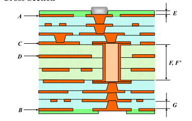
The next step is to drill holes into the substrate to form Microvia holes. These pores are usually very small, ranging from tens to hundreds of microns in diameter. After drilling is completed, fill the Microvia hole with filler material to ensure the reliability of the electrical connection within the hole.
Next, a circuit layer is printed on the surface of the substrate, usually using a photolithography process to transfer the pattern to the surface of the substrate. Then, unnecessary parts are removed through chemical etching, allowing the desired circuit pattern to be formed.
After the circuit pattern is completed, the Microvia Substrates need to be metallized to create conductive paths on the circuit pattern. Commonly used metallization methods include electroless copper plating or vacuum deposition of copper. Finally, the Microvia Substrates surface is coated to improve its corrosion resistance and weldability.
Manufacturing Microvia Substrates requires highly precise processing equipment and processes to ensure that the size and location of Microvia holes meet design requirements. This involves high-precision drilling and patterning processes.
During the manufacturing process of Microvia Substrates, environmental conditions need to be strictly controlled, including factors such as temperature, humidity, and dust. This helps ensure the stability of the production process and consistent product quality.
After each manufacturing step is completed, strict quality inspections are required to ensure that the quality of Microvia Substrates meets standards. This includes checking aspects such as aperture size, circuit pattern integrity, and metallization layer uniformity.
Manufacturing Microvia Substrates is a continuous improvement process that requires continuous optimization of processes and technologies to improve product quality and production efficiency. This requires manufacturers to continue R&D and experimentation to respond to changing market demands and technical challenges.
In the process of manufacturing Microvia Substrates, the above key steps and special processes and measures are key factors in ensuring the quality and performance of the final product. By strictly controlling each manufacturing step and using advanced technology and processes, high-quality, reliable Microvia Substrates can be produced to meet the needs of different electronic devices.
What are the specific manufacturing steps for Microvia Substrates?
The manufacturing process of Microvia Substrates involves multiple critical steps, each of which is critical and directly affects the quality and performance of the final product. Below we will introduce the specific manufacturing steps of Microvia Substrates in detail:
First, the substrate for manufacturing Microvia Substrates needs to be prepared. Glass fiber reinforced resin is usually selected as the substrate. A layer of special adhesive is then applied to the surface of the substrate to ensure a strong bond between subsequent layers.
Next, microvia holes are formed by drilling holes into the substrate using laser drilling or mechanical drilling techniques. The diameter of these Microvia holes usually ranges from tens to hundreds of microns. The holes are then filled with a conductive material, usually copper or another metal, to create a conductive path.
After the Microvia holes are filled, the next step is the printed circuit layer. The desired circuit pattern is formed by covering the surface of the substrate with a layer of conductive material, usually copper foil, and using chemical etching techniques to remove excess copper. This step determines the wire and connection structure of the Microvia Substrates.
Finally, metallization and surface coating are performed to protect the surface of Microvia Substrates and improve its corrosion resistance. By plating the surface with a layer of metal, such as nickel, gold or tin, and covering it with a protective polymer coating, Microvia Substrates ensure good electrical conductivity and mechanical strength, as well as durability and stability.
The above are the main steps of the manufacturing process of Microvia Substrates. Each step requires precision operations and strict quality control to ensure the performance and reliability of the final product. Through these steps, manufacturers can produce compliant Microvia Substrates to meet the needs of various electronic devices.
How much do Microvia Substrates cost?
The cost of Microvia Substrates depends on a variety of factors that directly impact the resources, technology, and labor costs required during the manufacturing and design process. Here are a few major factors that impact the cost of Microvia Substrates:
Board Selection: The cost of Microvia Substrates is affected by the type and quality of board selected. High-performance and specialty materials generally cost more than ordinary materials, such as materials such as polyimide (PI) and PTFE (polytetrafluoroethylene), which have excellent electrical properties and high temperature resistance, but are also priced accordingly.
Number of tiers and hierarchy: The cost of Microvia Substrates is closely related to its number of tiers and hierarchy. The more layers and the more complex the hierarchical structure of Microvia Substrates, the more difficult it is to manufacture and process, so the cost also increases.
Line width/space requirements: The line width/space requirements in Microvia Substrates also have a big impact on cost. Tighter line width/line spacing requirements require higher precision manufacturing equipment and processes, so costs will increase accordingly.
Pore size and density: Pore size and density in Microvia Substrates also affect cost. The requirement for smaller, denser apertures increases manufacturing costs because it requires more sophisticated machining processes and equipment.
Special process requirements: Some Microvia Substrates may require special processes, such as blind vias, buried vias, thick copper foil, etc. These process requirements will increase costs.
Production scale: Production scale also has a significant impact on the cost of Microvia Substrates. Large-scale production can reduce the cost per unit of product because fixed costs can be spread over more products.
To sum up, the cost of Microvia Substrates is affected by many factors, including board selection, number of layers and hierarchical structure, line width/line spacing requirements, aperture size and density, special process requirements, and production scale. Understanding these factors can help manufacturers and designers reasonably evaluate and control the cost of Microvia Substrates, thereby ensuring product quality and competitiveness.
What materials are Microvia Substrates made of?
Microvia Substrates are usually composed of a variety of materials, the most common of which include polyimide (PI), FR-4 glass fiber, and metal materials such as copper. Each material has unique characteristics and properties, and choosing the right material has a significant impact on the performance and reliability of Microvia Substrates.
Polyimide is a high-performance polymer material with excellent high-temperature stability, chemical stability and mechanical strength. Its low dielectric constant and low dielectric loss make it very popular in high frequency applications. In addition, PI materials also have excellent solvent resistance and fire resistance, making them suitable for application scenarios in complex environments.
FR-4 fiberglass is a common substrate material with good mechanical properties, heat resistance and electrical properties. It is composed of fiberglass cloth and epoxy resin, has high strength and rigidity, and is suitable for the manufacture of general electronic equipment. FR-4 fiberglass substrate is commonly used to manufacture thick Microvia Substrates.
Metal materials are mainly used for conductive layers and connection layers in Microvia Substrates. Copper is the most common metallic material with good electrical conductivity and processability, making it suitable for manufacturing the conductive paths and connection points of Microvia Substrates. In addition, copper has good corrosion resistance and thermal stability, ensuring the stability and reliability of Microvia Substrates under various environmental conditions.
Material selection has a direct impact on the performance and reliability of Microvia Substrates. Choosing the right materials ensures that Microvia Substrates have good electrical properties, thermal stability and mechanical strength, thereby improving the performance and reliability of electronic devices. For example, in high-frequency applications, choosing polyimide materials with low dielectric loss can reduce signal attenuation and distortion during signal transmission. In high-temperature environments, choosing materials with good heat resistance and chemical stability can ensure that Microvia Substrates can still work normally under extreme conditions.
To sum up, the material selection of Microvia Substrates is crucial, and a reasonable selection needs to be made based on specific application needs and performance requirements to ensure that the final product has excellent performance and reliability.
Who makes Microvia Substrates?
Microvia Substrates are produced by a range of specialized manufacturers, some of whom may be affiliates of electronic equipment manufacturers, while others specialize in PCB manufacturing. However, for those businesses looking for high-quality Microvia Substrates, it is crucial to choose an experienced and reputable manufacturer.
In this regard, many companies choose to rely on their own in-house resources to manufacture Microvia Substrates. This approach not only ensures comprehensive control over product quality and production processes, but also speeds up product development and market promotion. As a company with strong technical strength and rich experience, we do the same.
Our company has advanced production equipment and technical teams that can independently complete the design and manufacturing of Microvia Substrates. We focus on quality management and strictly follow international standards and industry norms to ensure that the Microvia Substrates produced have excellent performance and reliability.
As a professional Microvia Substrates manufacturer, we are committed to providing customers with customized solutions and can produce them according to customer needs and specifications. We have an efficient customer service team that can respond to customer needs in a timely manner and provide professional technical support.
In addition to manufacturing Microvia Substrates, we are also actively involved in technology research and development and innovation, and continue to promote the development and progress of the industry. By continuously improving the production process and technical level, we are committed to providing customers with better and more reliable Microvia Substrates products to meet their growing needs.
To sum up, our company is a Microvia Substrates manufacturer with rich experience and strong strength, and we are committed to providing customers with high-quality, reliable products and excellent services. We believe that through our efforts and unremitting pursuit, we will become your most reliable partner.
What are the five characteristics of great customer service?
In the Microvia Substrates manufacturing industry, providing excellent customer service is crucial, not only to enhance customer satisfaction but also to promote the establishment of long-term relationships. Here are five hallmarks of great customer service and how to get Microvia Substrates design and manufacturing services that meet your expectations:
The first characteristic of great customer service is prompt response to customer needs and questions. Microvia Substrates manufacturers should be able to respond to customer inquiries, provide quotes and resolve issues quickly and efficiently. Timely communication can help customers feel valued and establish a good cooperative relationship.
The second hallmark of great customer service is providing professional technical support and advice. Microvia Substrates manufacturers should have rich industry experience and professional knowledge and be able to provide customers with targeted technical consultation and solutions to help customers solve problems in the design and manufacturing process.
The third hallmark of great customer service is the provision of customized solutions. Microvia Substrates manufacturers should be able to tailor products and services to meet their customers’ needs and requirements, in order to meet their individual needs.
The fourth characteristic of excellent customer service is maintaining good communication and cooperation with customers. Microvia Substrates manufacturers should maintain close communication and collaboration with customers, keep abreast of customer needs and feedback, and jointly solve problems to ensure the smooth progress of the project.
The fifth characteristic of great customer service is providing after-sales support and service. Microvia Substrates manufacturers should be able to provide continuous after-sales support and services after product delivery to help customers solve subsequent problems and ensure product stability and reliability.
FAQS
What materials are used in Microvia Substrates?
Microvia Substrates are typically constructed using high-performance materials such as epoxy resins, fiberglass, copper foils, and various additives for enhanced electrical and mechanical properties. The choice of materials depends on the specific requirements of the application.
What factors influence the cost of Microvia Substrates?
The cost of Microvia Substrates is influenced by factors such as board size, layer count, complexity of the design, choice of materials, and manufacturing volume. Customized features and special requirements may also impact the overall cost.
Who manufactures Microvia Substrates?
Microvia Substrates are manufactured by specialized PCB fabrication companies with expertise in high-density interconnect technologies. These manufacturers utilize advanced equipment and processes to produce Microvia Substrates to precise specifications.
How can I ensure quality customer service when sourcing Microvia Substrates?
Quality customer service in sourcing Microvia Substrates involves timely communication, technical expertise, customization options, responsive support, and reliable post-sales assistance. Choosing a reputable manufacturer with a track record of delivering high-quality products and services is essential.
What are some common challenges associated with Microvia Substrates?
Common challenges related to Microvia Substrates include ensuring proper alignment and registration of microvias, controlling aspect ratios during laser drilling, optimizing plating processes for uniform copper deposition, and managing thermal issues in high-density designs.