 Professional Flip-Chip Packaging Substrate Supplier

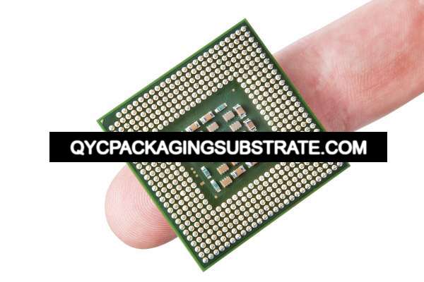
Microvias | Blind Vias PCB manufacturing. We use advanced Msap and Sap technology to do the Microvias HDI PCBs from 4 layer to 30 layers, the Minimum trace/spacing are 9um.
Microvias PCB (Printed Circuit Board) is an indispensable component of modern electronic equipment. Through its microvia technology, Microvias PCB provides high-density connections and optimized layout, making electronic products more compact and higher-performing. This article will delve into the manufacturing process of Microvias PCB to help readers fully understand its design, manufacturing and characteristics, and provide strong support for the development and production of electronic products.
What is Microvias PCB?
Microvias PCB (Printed Circuit Board) is a printed circuit board that has smaller and denser connection holes than traditional PCB, often called microvias. These microvias are typically less than 150 microns in diameter, allowing for higher connection density and more optimized layout. Microvias PCBs play a key role in modern electronic equipment. They not only provide the function of connecting electronic components, but also realize high-frequency, high-speed, and high-density circuit layout, making electronic products more compact, lightweight and with higher performance. .
In the past few decades, with the continuous development of electronic equipment and the increasing demand for intelligence, Microvias PCB has become an important part of the electronic manufacturing industry. They are widely used in fields such as communication equipment, computer hardware, medical equipment, automotive electronics, etc., providing strong support for electronic products in various fields.
One of the key features of Microvias PCBs is their high-density connectivity capabilities. Due to the smaller size of microvias, more connections can be made in a relatively small area, allowing for more compact circuit layouts. This makes Microvias PCBs particularly suitable for space-constrained or weight-critical applications such as mobile devices and drones.
In addition, Microvias PCB also has more optimized signal transmission characteristics. The introduction of micropores reduces the path length of signal transmission, reducing delay and distortion during signal transmission, thereby achieving higher signal quality and data transmission rate. This makes Microvias PCB ideal for high-frequency, high-speed electronic applications such as 5G communications equipment, high-performance computers and network equipment.
In general, the emergence and widespread application of Microvias PCB not only promotes the continuous progress and development of electronic equipment, but also provides a solid foundation for the promotion of innovation and technology. With the continuous evolution of technology and changing needs, the application prospects of Microvias PCB will be broader, injecting new vitality and power into the development of the electronics industry.
How to design Microvias PCB?
Designing Microvias PCB is a critical task, and its quality and performance directly affect the stability and reliability of the entire electronic product. Here are the key steps in designing Microvias PCBs to ensure high performance and reliability:
Determine design requirements: First, you need to clarify the functional requirements and performance indicators of the product. This includes determining the number of layers, layout, electrical characteristics, etc. of the circuit.
PCB layout planning: Carry out PCB layout planning according to design requirements. During the layout stage, the location of components, the direction of connection lines, and the placement of microvias need to be considered.
Choose the right CAD software: Use professional CAD software for PCB design, such as Altium Designer, Cadence Allegro, etc. These software provide rich design functions and tools to meet the needs of complex circuit design.
Draw the circuit diagram: Draw the circuit diagram according to the layout plan. When drawing a circuit diagram, you need to pay attention to maintaining good wiring principles, such as minimizing signal paths, separation of power lines and signal lines, etc.
Determine Microvias layout: Determine the location and number of Microvias based on circuit requirements and layout planning. Typically, Microvias are placed where high-density connections are required, such as underneath BGA packages.
Set Microvias parameters: Determine Microvias aperture, vertical spacing, vertical connector size and other parameters. These parameters need to be set appropriately based on the circuit design and PCB manufacturing process to ensure connectivity and reliability.
Microvias | Blind Vias PCB manufacturing
Consider thermal management: When designing Microvias PCB, you need to consider thermal management issues. Properly setting the location and layout of Microvias and adding heat dissipation design can effectively reduce the temperature of the circuit and improve the stability of the system.
Conduct simulation analysis: After the design is completed, conduct electrical simulation and signal integrity analysis. Through simulation analysis, the performance and stability of the circuit can be evaluated and the design can be optimized.
Improve design documents: Finally, improve design documents, including PCB layout diagrams, circuit diagrams, component lists, etc. Design documents are an important basis for PCB manufacturing and also facilitate subsequent production and maintenance work.
Through the above steps, a high-performance and reliable Microvias PCB can be designed to meet the needs of complex electronic products. During the design process, paying close attention to every detail to ensure the stability and reliability of the circuit is the key to successful design.
What is the manufacturing process of Microvias PCB?
The manufacturing process of Microvias PCB is a complex and precise process involving multiple critical steps, each step is crucial to ensure that the quality and performance of the final product meet the expected requirements.
Before manufacturing Microvias PCB, detailed design and planning first need to be carried out. This stage includes determining the number of layers of the circuit board, selection of board materials, layout and wiring, location and size of microvias, etc. Designers must consider the board’s end use and specific performance requirements to ensure the design is achievable and manufacturable.
The first step in manufacturing Microvias PCB is to convert the design into a graphical circuit board image and make a pattern making mold for the circuit board. This step usually uses photolithography technology to transfer the design pattern to the surface of the copper-clad substrate to form the required circuit pattern and microhole locations.
Next, the unnecessary copper is removed through etching technology, exposing the metal traces and microvia locations on the circuit board. After etching, microhole drilling is performed to penetrate the circuit board. This step requires a high degree of precision to ensure that the size and position of the micropores are exactly as designed.
After drilling the micropores, copper is plated inside the micropores through chemical methods to form a good conductive connection. Subsequently, the micropores are filled, usually using special filling materials or by adding metal into the micropores through electroplating methods. This step is critical to ensure the conductivity and reliability of the micropores.
During the final stages of manufacturing Microvias PCBs, surface treatments are performed to improve the board’s corrosion resistance and soldering performance. Common surface treatment methods include tin spraying, gold spraying, silver spraying, etc. After completing the surface treatment, strict inspection and testing are carried out to ensure that the circuit board meets the design requirements and quality standards, including visual inspection, electrical testing, solder joint inspection, etc.
Through the above key steps, Microvias PCB manufacturing process has completed the precise control of key processes such as circuit board design, processing, filling and surface treatment, ensuring that the quality and performance of the final product meet customer requirements and expectations.
What are the specific steps for Microvias PCB manufacturing?
The manufacturing process of Microvias PCB is a complex and precise process that requires multiple steps to ensure the high quality and reliability of the final product. The specific steps for manufacturing Microvias PCB will be introduced in detail below:
Substrate preparation: First, select a suitable substrate material, usually high-performance materials such as FR-4 or high-frequency materials. Then, the substrate is cut and cleaned to ensure the surface is flat and free of contamination.
Patterning: Use CAD software to design the pattern of Microvias PCB, including circuit layout and micro-hole locations. Then, photolithography is used to transfer the design pattern to the surface of the substrate, forming a conductive pattern.
Copper plating: Electroless copper plating is performed on the surface of the substrate to form a conductive layer. In this step, pay special attention to the copper plating of the microvias, ensuring that they are evenly covered with copper layers inside and outside to ensure good connectivity.
Microvia Drilling: Using laser drilling or mechanical drilling technology to drill holes into a substrate to form microscopic holes. These microvias, which typically have smaller diameters and higher densities, are used to connect different levels of circuitry.
Etching: The micro-holes formed by drilling are etched to remove the unnecessary copper layer, exposing the internal connections of the micro-holes.
Filling: Micropores are filled to ensure good electrical conductivity and mechanical strength. Commonly used filling materials include polyimide resin (PI) or polyamide (PAA).
Surface Treatment: The surface of Microvias PCB is treated to improve corrosion resistance and solderability. Common surface treatment methods include tin spraying, gold spraying, silver spraying, etc.
Final inspection: Conduct final inspection on the manufactured Microvias PCB, including appearance inspection, dimensional measurement, electrical performance testing, etc., to ensure that the product meets the design requirements and quality standards.
Through the above steps, the process of manufacturing Microvias PCB will ensure a high-quality finished product with excellent electrical performance and reliability. The application of these micro-hole technologies makes the design of electronic products more flexible and efficient, suitable for various high-density and high-performance application scenarios.
These steps are designed to provide readers with a comprehensive understanding of manufacturing Microvias PCB and help them better understand the manufacturing process and characteristics of Microvias PCB, thereby providing better support and guidance for the design and application of electronic products.
How much does Microvias PCB cost?
The cost of manufacturing Microvias PCBs is a complex and multifaceted consideration that is influenced by many factors. The following will introduce how the cost of manufacturing Microvias PCB is calculated and what factors are affected.
First of all, the cost of manufacturing Microvias PCB is usually calculated based on the following aspects:
Material cost: Material is an important component of the cost of PCB manufacturing. Microvias PCB usually requires high-performance substrate materials, such as FR-4, PTFE, etc. These materials are more expensive than traditional PCB materials.
Process cost: Manufacturing Microvias PCB requires a series of complex processes, such as patterning, etching, electroplating, etc. These processes require advanced equipment and technical support, thus increasing manufacturing costs.
Design complexity: The design complexity of Microvias PCB will directly affect the manufacturing cost. More complex designs typically require more processing steps and more advanced equipment, increasing costs.
Quantity and Size: The cost of manufacturing Microvias PCB also depends on the quantity of the order and the size of the PCB. Generally speaking, mass production can reduce costs, while larger size PCBs may require more materials and processing time, so the cost will increase accordingly.
Special requirements and technologies: If customers have special requirements or need to use advanced technologies, such as blind vias, buried vias, etc., these will increase manufacturing costs.
In addition to the above aspects, there are some other factors that may affect the cost of Microvias PCB, such as market competition, raw material price fluctuations, labor costs, etc.
To sum up, the cost of manufacturing Microvias PCB is a comprehensive consideration and needs to consider the influence of multiple factors. To reduce costs and increase competitiveness, customers and manufacturers need to consider these factors during the design phase and work closely with manufacturers to ensure that the final product is both compliant and cost-effective.
What materials are Microvias PCBs made of?
The manufacturing of Microvias PCBs involves selecting appropriate materials to meet high performance and reliability requirements. The following are the materials commonly used to manufacture Microvias PCBs:
FR-4 is one of the most commonly used substrate materials and has good electrical and mechanical properties. It is an inexpensive option and suitable for many standard applications, but there may be performance limitations for high frequency and high speed applications.
PTFE is a high-performance material with excellent dielectric properties suitable for higher frequency applications. It has the characteristics of low loss and low dielectric constant, and can meet circuit designs with high requirements for signal transmission quality.
RO materials are a class of materials specifically designed for high-frequency applications, with lower dielectric losses and higher signal transmission speeds. Common RO materials include RO4003C and RO4350B, etc., which are suitable for high-frequency circuit design such as wireless communications and radio frequency amplifiers.
High-speed sheets are a type of material specifically designed for high-speed digital signal transmission, with lower signal transmission loss and better signal integrity. These materials typically have higher glass transition temperatures (Tg) to ensure stability in high-temperature environments.
For some special applications, such as high-power electronic equipment or circuits with high heat dissipation requirements, metal substrates are an ideal choice. The metal substrate has excellent heat dissipation properties and can effectively transfer heat to the external heat sink.
Selecting the appropriate material depends on specific application requirements, including signal frequency, transmission speed, thermal management, etc. These factors must be taken into consideration when designing Microvias PCBs to ensure the final product has the required performance and reliability.
To summarize, Microvias PCBs are usually made from a variety of materials, each with specific characteristics and advantages to meet the requirements of different applications. When selecting materials, comprehensive considerations should be made based on specific design needs and performance requirements, and the most suitable material should be selected to achieve optimal performance and reliability.
Who makes Microvias PCBs?
In the manufacturing process of Microvias PCB, choosing the right supplier is crucial. For many companies, ensuring a partner has a high level of technical expertise and manufacturing capabilities is critical. So, who makes Microvias PCBs? For our company, we own and operate our own dedicated manufacturing facilities to ensure our customers receive the highest quality products.
As a leading electronics manufacturing service provider, we have advanced production equipment and technical teams to meet our customers’ various needs. Our factory is equipped with the latest CAD software and lithography equipment to support the development and production of complex Microvias PCB designs. From the selection of raw materials to the manufacturing of final products, our manufacturing processes strictly comply with international standards and undergo strict quality control and inspection.
In addition to our in-house manufacturing capabilities, we work with multiple quality material suppliers to ensure that the materials used in our Microvias PCBs are of the highest quality. This includes high-performance substrate materials, conductive materials and surface treatment materials to ensure the performance and reliability of the final product.
Our customers can rest assured that we not only provide high-quality products, but also provide professional technical support and customer service. Our team is always available to provide customers with assistance and solutions, and ensure they receive prompt and attentive service throughout the entire manufacturing process.
Anyway, who makes Microvias PCBs? For us, the answer is: our company. Based on our own factory and professional team, we provide customers with high-quality and reliable Microvias PCBs to meet their growing needs and challenges.
What are the five characteristics of great customer service?
Providing excellent customer service is key to ensuring customer satisfaction and maintaining long-term business relationships. Listed below are five key features to ensure customers receive the best possible service experience:
Prompt Response: Responding quickly to customer questions, concerns or needs is critical. Whether by phone, email or online chat, respond to customer inquiries in a timely manner and demonstrate customer care. Quick response can effectively reduce customer waiting time, enhance customer confidence in service, and improve customer satisfaction.
Expertise: Customers want to deal with professionals who know their stuff, can solve their problems and provide valuable advice. Provide training and ongoing learning opportunities to ensure the customer service team remains up-to-date on product knowledge and industry trends. By providing professional technical support and consulting services, we build customer trust in the company, thereby enhancing customer loyalty.
Customized Solutions: Every customer has unique needs and challenges, so providing customized solutions is key to increasing customer satisfaction. Through in-depth understanding of customers’ business and needs, we tailor products and services to meet their specific requirements. Customized solutions can improve product adaptability and performance, enhance customer experience, and promote the establishment of long-term partnerships.
Good communication: Establishing good communication channels is the basis for maintaining a good relationship with customers. Maintain close communication with customers, communicate important information and progress in a timely manner, and ensure customers understand the status of their projects or orders. Listen to customer feedback and suggestions, promptly solve problems and improve services to improve customer satisfaction and loyalty.
After-sales support: Good after-sales support is key to improving customer satisfaction and maintaining customer relationships. Solve customer problems and complaints in a timely manner, provide technical support and maintenance services, and ensure customer satisfaction with products and services. Establish a complete after-sales service system to provide customers with continuous support and assistance, and enhance customers’ trust and loyalty to the company.
To sum up, timely response, expertise, customized solutions, good communication and after-sales support are the five key characteristics of providing excellent customer service. By focusing on these aspects, companies can build good customer relationships, improve customer satisfaction, and achieve continued business growth and development.
FAQS
What factors influence the cost of Microvias PCBs?
The cost of Microvias PCBs is influenced by factors such as board size, number of layers, complexity of the design, materials used, and manufacturing technology required. High-density designs with smaller vias and finer traces typically incur higher manufacturing costs.
How do you select a reliable manufacturer for Microvias PCBs?
When selecting a manufacturer for Microvias PCBs, it’s essential to consider factors such as experience, capabilities, quality certifications, and customer reviews. A reliable manufacturer will have a track record of producing high-quality PCBs and will be able to meet your specific requirements.
What are the main challenges in Microvias PCB manufacturing?
Challenges in Microvias PCB manufacturing include maintaining tight tolerances for small diameter vias, ensuring uniform plating and filling of vias, and controlling impedance and signal integrity in high-frequency designs. Addressing these challenges requires advanced manufacturing techniques and quality control measures.
How can I ensure the reliability of Microvias PCBs in my application?
Ensuring the reliability of Microvias PCBs involves thorough testing and inspection during the manufacturing process, as well as validation testing in the application environment. It’s essential to work closely with your PCB manufacturer to identify potential reliability issues and implement appropriate design and manufacturing solutions.