 Professional Flip-Chip Packaging Substrate Supplier

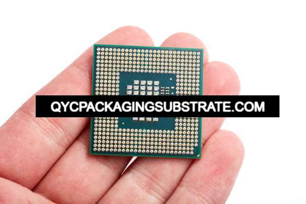
Microvias PCB manufacturing. HDI High speed and high frequency material Microvias PCBs, and HDI BGA packaging substrate Vendor. We offer Microvias PCB from 4 layer to 30 layers. the best smallest via holes size are 2mil(50um). some are 3mil and 4mil is the standard laser via holes.
In the field of modern electronics, Microvias PCB has become a vital technology, which not only promotes the miniaturization and performance improvement of electronic equipment, but also provides unlimited possibilities for innovation. However, for beginners, the complexity of Microvias PCB manufacturing can be daunting. From design to manufacturing to cost considerations, this article will delve into all aspects of Microvias PCB to help you easily harness the essence of this technology.
What is Microvias PCB?
Microvias PCB (Printed Circuit Board) is a printed circuit board that plays a vital role in the field of modern electronics. Compared with traditional printed circuit boards, Microvias PCBs have a distinctive feature, and that is that they have tiny drilled holes, called Microvias. These tiny holes connect different layers of the PCB, making connections between electronic devices more compact and efficient.
The emergence of Microvias PCB is mainly in response to the trend of increasingly miniaturized electronic equipment. In compact devices, space is a precious resource, and Microvias PCB makes it possible to achieve more circuit connections in a limited space through its high-density interconnection characteristics.
These Microvias are typically manufactured using laser drilling technology and typically range in diameter from tens to hundreds of microns. They are precisely arranged on the surface of the PCB and connect different circuit layers to achieve electrical connections between electronic devices.
Microvias PCB manufacturing
Due to the special design of Microvias PCBs, they usually have higher wiring density and smaller size. This makes them the first choice for many modern electronic devices, especially for space-critical applications such as smartphones, tablets, wearables, etc.
In general, Microvias PCB is not just a printed circuit board, but also a product of technological innovation. It provides strong support for the development of modern electronic equipment and promotes the continuous progress and development of the electronics industry.
How to design Microvias PCB?
Designing Microvias PCB is a complex and critical process that requires careful planning and consideration of various factors. The following are key considerations when designing Microvias PCBs:
Microvias PCBs usually have multi-layer structures, so stack-up design is crucial. The designer needs to determine the number of layers of the board and how each layer will function and connect. Through reasonable stacking design, signal transmission and electrical performance can be optimized to the greatest extent.
In Microvias PCB design, the size of the pads and apertures directly affect the connection quality and stability of the pads and microvias. Designers need to size pads and apertures based on factors such as current flow, heat, and mechanical strength to ensure board reliability and performance.
Microvias PCB routing constraints are one of the important considerations during the design process. Wiring constraints include minimum distance, minimum aperture, minimum line width and other specifications to ensure the stability and reliability of wiring. Designers need to develop appropriate routing constraints based on circuit requirements and manufacturing process constraints.
Designing Microvias PCBs usually requires the use of professional circuit design software such as Altium Designer or Cadence Allegro. These software provide rich features and tools to effectively support complex design requirements. Designers can use these software for circuit layout, routing, simulation and verification to ensure the accuracy and reliability of their designs.
When designing Microvias PCB, designers need to consider the above factors and work closely with manufacturers to ensure that the final design meets the requirements and can be manufactured smoothly. Through careful design and cooperation, Microvias PCB is able to achieve optimal performance and reliability, providing strong support for the development of electronic devices.
What is the manufacturing process of Microvias PCB?
The Microvias PCB manufacturing process is a complex and precise process designed to ensure the reliability and performance of the final product. The following are the key steps in Microvias PCB manufacturing:
The first step in manufacturing Microvias PCB is to prepare the substrate. This includes selecting an appropriate substrate material, typically FR-4 or other high-performance material, and ensuring its surface is smooth and clean for subsequent process steps.
Microvias are tiny holes that connect different layers, and their drilling is one of the key steps in Microvias PCB manufacturing. Laser drilling technology is often used to create tiny and precise apertures to enable high-density routing and interconnection.
After drilling Microvias, a thin layer of copper needs to be deposited on the walls and bottom of the hole. This step is called copper deposition, which helps improve the conductivity and reliability of Microvias and provides a good conductive foundation for subsequent line laying.
Surface treatment is the final step in Microvias PCB manufacturing and is designed to protect the board surface and improve soldering reliability. Common surface treatment methods include tin spraying, gold spraying, silver spraying, etc. These methods can prevent oxidation, improve welding performance, and increase the corrosion resistance of the board.
For complex Microvias PCB designs, sequential lamination technology may be used. This technology allows alternating copper foil and substrate material between multiple layers and forming Microvias in the appropriate locations on each layer, allowing for higher routing density and design flexibility.
Every step of the Microvias PCB manufacturing process must be precisely controlled and executed to ensure that the final product meets design specifications and has good performance and reliability. Through reasonable design and precise manufacturing processes, Microvias PCB has become an indispensable part of modern electronic equipment, promoting continuous technological progress and innovation.
How to make Microvias PCB?
Manufacturing Microvias PCBs is a complex and sophisticated process that requires specialized skills and a high degree of precision. First, the design files need to be sent to a PCB manufacturer that specializes in Microvias PCB manufacturing. These manufacturers have advanced equipment and technology that can handle microscopic features and ensure high quality and accuracy of their products.
In the manufacturing process, the first step is to prepare the substrate. This involves selecting an appropriate substrate material, typically FR-4 or a similar high-performance material. Then, laser drilling technology is used to form tiny holes, called Microvias, on the substrate. These Microvias are used to connect circuits between different layers.
Next comes copper deposition and plating. Copper is deposited on the Microvias and surfaces to create conductive pathways and enhance circuit connectivity and reliability. Then, surface treatment is performed to protect the copper layer from corrosion and provide a good soldering surface.
Quality control measures are critical throughout the entire manufacturing process. Manufacturers implement strict quality control procedures, including checking process parameters at each step and the finished quality of the final product. These measures ensure the integrity and reliability of Microvias PCBs to meet customer needs and specifications.
Overall, manufacturing Microvias PCB is a comprehensive process that requires a high degree of expertise and technology. By working with experienced PCB manufacturers, you can ensure the highest level of product quality and performance to meet the high-density, high-performance circuit board demands of modern electronic equipment.
What are the cost considerations for Microvias PCBs?
Microvias PCB cost considerations are very important as this directly affects the feasibility and cost-effectiveness of the project. Let’s take a deeper look at these factors.
First, the board size of Microvias PCB is a key factor. Larger boards usually require more materials and manufacturing processes, so the cost is relatively higher. While smaller boards may cost less, they require greater manufacturing precision.
Secondly, the number of layers will also affect the cost of Microvias PCB. Multilayer boards require more steps and complex manufacturing processes, so the cost is usually higher. In comparison, double-sided or four-layer boards may cost less to manufacture.
Microvias density is another important factor. Dense Microvia layouts require more manufacturing steps and precision machining, leading to higher costs. Conversely, lower-density Microvias layouts may reduce costs.
Finally, material specifications also have an impact on cost. High-performance materials typically cost more, but offer advantages in providing better performance and reliability. Choosing the right materials can control costs to a certain extent and ensure that the requirements of the project are met.
Although Microvias PCBs may cost slightly more to manufacture than traditional PCBs, the space savings and performance improvements they bring often justify the investment. Through precise design and efficient manufacturing processes, costs can be maximized and satisfactory results ensured.
To summarize, understanding Microvias PCB cost considerations is critical to the success of your project. By carefully evaluating factors such as board size, layer count, Microvias density and material specifications, a suitable manufacturing solution can be developed to achieve the best balance of cost and performance.
What materials are used in Microvias PCB?
Microvias PCB is a critical electronic component whose design and manufacture are critical to the performance and reliability of modern electronic devices. In Microvias PCB manufacturing, choosing the right material is crucial because the quality of the material directly affects the performance and stability of the PCB. The materials commonly used in Microvias PCB will be introduced in detail below.
First, Microvias PCBs are typically made from high-performance materials, the most common of which is FR-4. FR-4 is a glass fiber reinforced epoxy resin material with good electrical properties and mechanical strength. In addition, FR-4 also has a high glass transition temperature and can maintain stability in high-temperature environments, ensuring that Microvias PCBs can operate reliably under harsh working conditions.
In addition to FR-4, other advanced substrate materials such as Rogers or Isola are also available for specific applications. Rogers is a high-frequency circuit board material with excellent dielectric properties and low loss, suitable for electronic equipment with high frequency and high-speed transmission. Isola is a high-performance substrate material with excellent thermal stability and mechanical strength, and is suitable for applications with high requirements on ambient temperature and mechanical stress.
Choosing the right substrate material is critical to Microvias PCB performance. In addition to considering the electrical properties and mechanical strength of the material, factors such as its heat resistance, corrosion resistance, and processability also need to be considered. Through reasonable selection of materials, Microvias PCB can be ensured to work stably and reliably in various working environments.
In general, Microvias PCB material selection is a comprehensive consideration process and needs to be selected based on specific application needs and performance requirements. Choosing the right material can improve the performance and reliability of PCB and provide a solid guarantee for the stable operation of electronic equipment.
Who are the key players in Microvias PCB manufacturing?
In the Microvias PCB manufacturing ecosystem, key players include PCB manufacturers, raw material suppliers, and equipment suppliers. Internally, supplier selection is critical to the quality and performance of Microvias PCBs. These key players are detailed below.
PCB manufacturer is one of the core players in Microvias PCB manufacturing. These companies have advanced equipment and technology capable of handling tiny apertures and high-density wiring. They are responsible for converting design files into actual PCBs and ensuring product reliability through strict quality control. Excellent PCB manufacturers have rich experience and expertise and can provide customized solutions according to customer needs.
For Microvias PCB manufacturers, choosing the right raw materials is crucial. These raw materials include substrate materials, copper foil, coating materials, etc. High-quality raw materials can ensure the stability and performance of PCB, which is especially critical for the manufacturing of fine pores. Therefore, PCB manufacturers need to establish strong cooperative relationships with reliable raw material suppliers to ensure product quality and delivery time.
Equipment suppliers provide PCB manufacturers with the necessary production equipment and tools. These equipment include laser drilling machines, copper plating line equipment, surface treatment equipment, etc. Choosing high-performance equipment can improve production efficiency and product quality, so PCB manufacturers need to cooperate with leading equipment suppliers to maintain competitive advantages in technology updates and production capabilities.
As one of the key players in Microvias PCB manufacturing, our company is committed to providing high-quality raw materials and professional technical support. We have advanced production equipment and rich industry experience to meet customers’ various needs for Microvias PCBs. We have established close cooperative relationships with excellent PCB manufacturers and equipment suppliers, and are committed to promoting the development and innovation of Microvias PCB manufacturing technology.
By partnering with us, customers receive reliable products and quality service to achieve their electronic product performance and reliability goals. We will continue to work hard to provide customers with the best solutions and become a reliable partner in the field of Microvias PCB manufacturing.
What are the characteristics of excellent Microvias PCB manufacturing services?
Excellent Microvias PCB manufacturing services are the key to customer success, and this success depends not only on the quality of the product itself, but also on the key attributes demonstrated by the service provider during the manufacturing process. Below is a detailed description of these qualities:
Microvias PCB manufacturing involves tiny sized drill holes and traces, so precision is crucial. An excellent manufacturing service provider should have advanced production equipment and precise manufacturing processes to ensure accurate manufacturing of Microvias and strict tolerances. Through precision control and monitoring, they are able to ensure that the size and location of each Microvias meet design specifications, guaranteeing the reliability and performance of the final product.
Microvias PCB manufacturing involves complex design and material selection. An excellent manufacturing service provider should have extensive industry experience and expertise and be able to handle a variety of complex design requirements and special material needs. They should be able to provide professional advice and find innovative solutions when faced with challenges to ensure the final product meets customer requirements and expectations.
In the Microvias PCB manufacturing process, timely communication and support are crucial. A good manufacturing service provider should be able to maintain close contact with customers and respond promptly to their needs and questions. They should provide clear and concise updates on project progress and provide technical support and solutions when needed. Through active communication and collaboration, they are able to build trust and partnership with their clients.
Quality is at the core of Microvias PCB manufacturing. An excellent manufacturing service provider should implement strict quality control measures to ensure that every aspect of the product meets quality standards and industry norms. They should conduct comprehensive inspections and tests to ensure that each Microvias meets or exceeds customer quality requirements. Through continuous quality monitoring and improvement, they are able to deliver high-quality products that provide lasting value to their customers.
Customer needs are diverse, so flexibility is another important attribute of a good manufacturing service provider. They should be able to flexibly respond to changes in customer demand and adjust production plans and processes in a timely manner. They should be able to customize production solutions to meet customers’ specific requirements and custom specifications. Through flexible production capabilities, they are able to provide customers with personalized solutions and achieve win-win partnerships.
In summary, a good Microvias PCB manufacturing service provider should possess key attributes such as precision, expertise, responsiveness, quality assurance and flexibility to meet customer needs and achieve continued business success. By actively responding to challenges and continuously improving their capabilities and standards, they can stand out in a highly competitive market and win the trust and support of customers.
FAQS
Can Microvias PCBs be used in high-frequency applications?
Yes, Microvias PCBs are well-suited for high-frequency applications due to their ability to minimize signal distortion and impedance mismatch. By reducing parasitic capacitance and inductance, Microvias technology enables improved signal integrity and enhanced transmission line performance. Designers can leverage Microvias PCBs to achieve reliable signal propagation and precise control over signal characteristics in high-speed communication systems, RF devices, and other demanding applications.
What are the advantages of using Microvias PCBs?
Microvias PCBs offer several advantages, making them an attractive choice for various electronic applications. Firstly, their miniature size allows for higher routing density, enabling more components to be packed into a smaller footprint. This is particularly advantageous for compact electronic devices such as smartphones, wearables, and IoT gadgets. Secondly, Microvias facilitate shorter signal paths, reducing signal distortion and improving signal integrity, which is critical for high-speed and high-frequency circuits. Additionally, Microvias PCBs offer enhanced thermal management due to their efficient heat dissipation properties, ensuring reliable performance even in thermally challenging environments. Overall, the advantages of Microvias PCBs translate into improved functionality, performance, and reliability for electronic products.
What limitations does Microvias PCB technology have?
While Microvias PCBs offer numerous benefits, they also come with certain limitations that engineers and designers need to consider. One limitation is the increased complexity of manufacturing and assembly processes associated with Microvias PCBs, which may result in higher production costs and longer lead times compared to traditional PCBs. Moreover, Microvias PCBs may exhibit reduced reliability in high-temperature environments due to the smaller size of the vias and increased susceptibility to thermal stress. Compatibility issues with certain assembly processes, such as soldering techniques, may also arise due to the unique characteristics of Microvias PCBs. Despite these limitations, careful design, material selection, and manufacturing practices can help mitigate potential challenges associated with Microvias PCB technology.
How can I ensure the reliability of Microvias PCBs?
Ensuring the reliability of Microvias PCBs requires attention to several key factors throughout the design, fabrication, and assembly processes. Firstly, adherence to best practices in PCB design, including proper layout, routing, and via placement, is essential to minimize signal integrity issues and ensure electrical reliability. Secondly, selecting high-quality materials with suitable thermal and mechanical properties is crucial for meeting reliability requirements, especially in demanding operating conditions. Additionally, partnering with reputable PCB manufacturers with expertise in Microvias technology and implementing robust quality control measures can help ensure the integrity and reliability of Microvias PCBs. Regular testing and validation procedures, including thermal cycling and reliability testing, can further verify the performance and durability of Microvias PCBs in real-world applications.