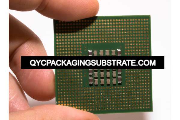
 Professional Flip-Chip Packaging Substrate Supplier

Minimum Pad Clearance PCB manufacturing , Ultra-small bump pitch, ultra-small trace and spacing package substrates and LED PCBs Vendor.
In today’s digital age, printed circuit boards (PCBs) are the unsung heroes that support our daily devices. From smartphones to smartwatches, PCBs are the invisible connectors. However, a deeper dive into the world of PCB manufacturing reveals a critical aspect that is often overlooked: minimum pad clearance. In this fascinating field, what is the secret behind Minimum Pad Clearance PCB manufacturing? Let us uncover its mystery together and explore its technical essence.
What is the minimum pad gap?
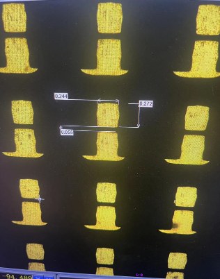
In the PCB (Printed Circuit Board, printed circuit board) design and manufacturing process, the minimum pad gap is a crucial indicator. It refers to the minimum distance between the edge of a pad on a PCB and any other nearby conductive elements (such as circuit traces, other pads, etc.). Ensuring this spacing is critical to the integrity and reliability of the circuit.
First, let’s understand why minimum pad clearance is so important. On the PCB, the pads perform the important tasks of connecting electronic components and circuit tracing. However, if the distance between pads or between pads and other conductive elements is too small, the risk of short circuits increases. Short circuits can cause circuits to malfunction or even damage electronic equipment. In addition, too small a gap may cause signal interference or cross-interference, thus affecting the performance and stability of the circuit.
Minimum Pad Clearance PCB manufacturing
Therefore, several factors need to be considered in determining the minimum pad gap. The first is pad size and layout. The size and spacing of the pads should be large enough to ensure that they do not accidentally come into contact with other conductive elements when soldering components. Second is the distance between circuit traces and other elements. The distance between these elements should be large enough to prevent short circuits and signal interference.
During the PCB design stage, engineers usually use professional design software to simulate and optimize pad layout and gaps. They follow industry standards and best practices to ensure pad gaps meet specifications and ensure circuit reliability and stability.
In the PCB manufacturing process, achieving minimum pad gaps requires manufacturers to adopt advanced manufacturing technology and precision processes. For example, they might use laser drilling technology to ensure the precise placement and size of pads to reduce interference with other elements. In addition, high-resolution imaging technology can help manufacturers inspect and verify that pad gaps meet specification requirements.
Overall, minimum pad clearance plays a vital role in PCB design and manufacturing. By ensuring proper distances between pads and from other conductive elements, we ensure the stability and reliability of electronic circuits, ensuring proper operation and long-term performance of the device.
Minimum Pad Clearance PCB
How to achieve minimum pad clearance in PCB design?
Achieving minimum pad clearance in PCB design is a task that requires intense focus and precision. Engineers must carefully consider every detail to ensure that the final design meets strict clearance requirements and effectively prevents possible short circuits and signal interference.
First, designers need to carefully lay out components and traces. This means that when placing various electronic components on a PCB, you must consider their interactions with each other and their positional relationship with other surrounding components. With proper layout, you can minimize crossings between pads and ensure there is enough space for each pad to prevent any unnecessary contact.
Second, engineers need to carefully plan the routing. When connecting wires between electronic components, you must ensure that the trace paths are clear and avoid crossovers and overlaps. Not only does this reduce potential signal interference, it also ensures that any possible issues are easily identified and troubleshooted if necessary.
The key point is that there must be enough spacing between the pads to prevent short circuits. This means that during the layout and routing process, designers must follow strict specifications to ensure there is enough space around each pad to accommodate the minimum pad gap requirements. This may require multiple adjustments and optimizations between component placement and routing to ensure the best design results.
Additionally, using PCB design software can greatly simplify this process. These software often provide design rule checking (DRC) capabilities that help designers quickly identify potential layout and routing issues and provide recommendations to resolve them. By leveraging these tools, designers can more efficiently achieve minimum pad gaps while ensuring design accuracy and consistency.
All in all, achieving PCB design with minimum pad clearance requires the focus and skill of the engineer. Through careful layout, route planning, and the use of appropriate design tools, designers can ensure that the final design meets strict clearance requirements and ensures circuit reliability and stability.
How to manufacturing a Minimum Pad Clearance PCB?
In the PCB manufacturing process, achieving minimum pad gaps requires precise and specialized techniques. Advanced manufacturing technologies, such as laser drilling and high-resolution imaging, are key to achieving this goal. Laser drilling technology allows manufacturers to create tiny, precise holes in PCBs that are used to connect different levels of circuitry. The precise location and size of these holes is critical to ensuring minimum pad clearance. High-resolution imaging technology can accurately detect and measure the spacing between pads on the PCB surface to ensure that it meets specifications.
In addition to laser drilling and high-resolution imaging technology, manufacturers also rely on precision machining equipment and sophisticated processes. During the PCB manufacturing process, various steps such as substrate preparation, copper foil etching, printing, drilling and surface treatment must be strictly controlled to ensure that the final product meets the design specifications. Particularly in manufacturing steps involving pads, manufacturers must ensure that any errors or deviations are detected and corrected promptly to prevent deviations from gap specifications.
Powered by these technologies and processes, manufacturers are able to produce PCBs with ultra-fine features that not only meet minimum pad gap requirements but also meet the complexity needs of a variety of applications. For example, for high-density circuit boards, manufacturers can leverage these advanced technologies to achieve more compact layouts and smaller pad gaps, thereby improving board performance and reliability.
Overall, achieving PCB manufacturing with minimum pad gaps requires manufacturers to have advanced technology and strict quality control processes. Through continuous improvement and innovation, manufacturers are able to meet increasingly stringent design requirements and provide customers with PCB products of high quality, reliability and excellent performance.
What is the cost of minimum pad clearance?
Although achieving minimum pad clearance adds some complexity to the PCB manufacturing process, as technology continues to advance, this goal is easier to achieve and more cost-effective than ever before. As manufacturers take advantage of economies of scale and process optimization, they are able to minimize costs without compromising quality.
First, advances in technology provide more options and solutions for achieving minimum pad gaps. Modern PCB manufacturing technology includes high-precision machine control, advanced photolithography, and sophisticated material handling methods. The introduction of these technologies allows manufacturers to more precisely control the gaps between pads, thereby reducing manufacturing costs.
Secondly, the advantages of economies of scale make it more economical to mass-produce PCBs with minimal pad gaps. As manufacturing quantities increase, fixed costs can be spread over more products, lowering the cost of production per unit. This allows the cost per PCB to be kept within reasonable limits even during complex manufacturing processes that achieve minimal pad gaps.
In addition, process optimization also plays a key role. Manufacturers have further reduced manufacturing costs by improving production processes, increasing efficiency and reducing scrap rates. For example, optimized processes can reduce material waste and improve production efficiency, thereby reducing production costs. This process optimization makes PCB manufacturing with minimal pad gaps more cost-effective.
Overall, while achieving minimum pad gaps may add complexity to the manufacturing process, advances in technology, advantages in economies of scale, and process optimization allow manufacturers to minimize costs without compromising quality. This opens new possibilities for wider application of minimal pad gap PCBs and drives the development and innovation of electronic devices.
What materials are Minimum Pad Clearance PCB made of?
Minimum pad gap PCBs typically feature a range of high-quality materials to ensure their reliability, durability and performance. Among them, FR-4 substrate and copper foil with precise thickness specifications are one of the most common choices.
FR-4 substrate is a very popular substrate material composed of fiberglass and epoxy resin. This material has excellent mechanical strength and thermal stability, resisting temperature changes and environmental influences, while providing stable electrical properties. The FR-4 substrate also has good insulating properties, which can effectively prevent short circuits across pad gaps, and provides good mechanical support to help protect electronic components on the PCB from mechanical stress.
In addition to the substrate material, the choice of copper foil is also crucial. In minimum pad gap PCB manufacturing, copper foil must have precise thickness specifications to ensure circuit stability and reliability. As the material of the conductive layer, copper foil is responsible for transmitting current and signals, so its quality directly affects the performance of the PCB. By precisely controlling the thickness of the copper foil, manufacturers can ensure that the gaps between pads meet specifications and maintain good conductivity of the circuit.
Additionally, other materials such as pad overlays and solder masks may be used in minimum pad gap PCB manufacturing. Pad coverage, usually in the form of solder film or spray tin, is used to protect the pad surface from oxidation and corrosion while providing a good soldering surface. Solder mask is used to cover the PCB surface to prevent short circuits and protect circuit components. These additional materials play a key role in ensuring minimum pad gap PCB stability and reliability.
In summary, material selection for minimum pad gap PCB is critical, and high-quality materials are required to ensure circuit performance and reliability. FR-4 substrates and copper foil with precise thickness specifications are among the most commonly used materials. They provide the PCB with good mechanical support, stable electrical properties and reliable conductivity to meet strict clearance requirements and enable circuits to be Excellent performance in a variety of applications.
Who is the supplier of minimum pad gap PCB?
In the complex field of PCB manufacturing, finding a reliable supplier is crucial. For minimum pad gap PCB, it is especially important to choose a professional and reliable supplier. In this field, our company takes pride in being one of the most trustworthy suppliers.
Professional Experience: We have over 10 years of PCB manufacturing experience, specializing in producing minimum pad gap PCBs. Our team consists of experienced engineers and technical experts who can meet various customer requirements.
Advanced Technology: We invest in advanced manufacturing equipment and technology, including high-precision laser drilling and precision imaging systems, to ensure PCBs are produced to the most stringent specifications.
Quality Assurance: We strictly implement the quality management system and conduct strict monitoring and inspection in every aspect from raw material procurement to production process to ensure stable and reliable product quality.
Customized services: We can provide customized solutions based on customers’ specific needs, including PCBs of different sizes, layers and materials, as well as specific pad gap requirements.
Timely delivery: We have efficient production processes and flexible production capabilities, which can deliver customer orders in time to ensure the smooth progress of customer projects.
Our company has always taken customer satisfaction as its primary goal. Our customers are spread across all walks of life, including communications, medical, aerospace and other fields. They choose us as their minimum pad gap PCB supplier because of our reliability, quality and professional service.
As a supplier of minimum pad gap PCBs, we are committed to providing our customers with high quality, reliability and customized solutions. Our professional experience, advanced technology, quality assurance and customized services make us the preferred partner of our customers. When you choose us, you can trust us with your PCB manufacturing needs and we will serve you wholeheartedly to achieve your project goals.
What are 5 qualities of a good customer service?
In the world of minimum pad gap manufacturing, excellent customer service is paramount. Manufacturers must demonstrate the following five qualities to ensure customer needs are addressed promptly and efficiently:
Manufacturers should respond quickly to customer inquiries, questions or complaints. Responsiveness means responding to emails, answering phone calls, or responding to online messages in a timely manner so customers feel their concerns are taken seriously.
Manufacturers must have in-depth knowledge and expertise regarding the minimum pad gap manufacturing process. This includes a thorough understanding of design, materials, workmanship and industry standards to be able to provide customers with accurate and useful information.
Understanding your customers’ needs, concerns and challenges is key to building great customer relationships. Manufacturers should demonstrate empathy and connect emotionally with customers to ensure they feel understood and supported.
In a fast-paced manufacturing environment, things can change at any time. Manufacturers must be adaptable and able to flexibly adjust plans and processes to meet customer needs and make timely adjustments when necessary to resolve issues.
Clear, accurate and timely communication is critical to building good customer relationships. Manufacturers should maintain open lines of communication and ensure smooth flow of information to customers. Effective communication can help prevent misunderstandings and dissatisfaction and strengthen trust and partnership between manufacturers and customers.
By demonstrating qualities such as responsiveness, knowledge, compassion, adaptability, and effective communication, manufacturers can ensure customers receive the best service and support during their minimum pad gap manufacturing process. These qualities not only enhance customer satisfaction, but also build long-term, strong customer relationships, laying a solid foundation for business success and growth.
FAQ
How can manufacturers ensure consistent quality in Minimum Pad Clearance PCBs?
Consistent quality in Minimum Pad Clearance PCBs is achieved through rigorous quality control measures throughout the manufacturing process. This includes comprehensive inspection and testing procedures to verify compliance with clearance specifications and identify any defects or irregularities. Additionally, manufacturers may implement continuous improvement initiatives to optimize manufacturing processes and enhance product quality. By prioritizing quality assurance and implementing robust quality management systems, manufacturers can deliver Minimum Pad Clearance PCBs that meet the highest standards of reliability and performance.
What are the typical clearance requirements for Minimum Pad Clearance PCBs?
Clearance requirements for Minimum Pad Clearance PCBs can vary depending on several factors, including the specific application, the complexity of the design, and the capabilities of the manufacturing process. However, industry standards generally dictate minimum clearance distances ranging from a few mils to tens of mils. These requirements ensure that there is sufficient space between adjacent conductive elements on the PCB to prevent short circuits and signal interference, thereby maintaining the integrity and reliability of the electronic circuits.
How does Minimum Pad Clearance impact signal integrity?
Minimum Pad Clearance plays a crucial role in preserving signal integrity within a PCB. By maintaining adequate spacing between pads and other conductive elements, Minimum Pad Clearance helps minimize the risk of signal distortion and crosstalk. When signals travel through the traces on a PCB, interference from neighboring conductive elements can lead to signal degradation or corruption. However, by adhering to Minimum Pad Clearance specifications, engineers can mitigate these risks and ensure reliable signal transmission throughout the circuit.
Are there any environmental considerations associated with Minimum Pad Clearance PCB manufacturing?
Yes, environmental considerations are an important aspect of Minimum Pad Clearance PCB manufacturing. As the electronics industry strives for sustainability and eco-friendliness, manufacturers are increasingly adopting environmentally conscious practices throughout the manufacturing process. This includes using lead-free soldering materials to reduce hazardous waste, implementing recycling programs to minimize environmental impact, and adhering to regulatory standards for emissions and waste disposal. By incorporating these practices into Minimum Pad Clearance PCB manufacturing, companies can contribute to a greener and more sustainable future while still delivering high-quality products to their customers.