 Professional Flip-Chip Packaging Substrate Supplier

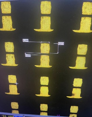
Minimum Trace&Clearance PCB manufacturing. High speed and high frequency HDI PCBs Vendor. we offer the PCB Minimum Trace&Clearance with 30um/30um, when we use the ABF base materials. we can do the Minimum Trace&Clearance with 9um/9um.
In the world of modern electronics, printed circuit boards (PCBs) are crucial, and they are the cornerstone of countless innovations. In PCB design and manufacturing, there is one crucial consideration: minimum traces and clearances. In this comprehensive guide, we will reveal the complexities of minimum trace and clearance PCB manufacturing, clarifying its importance and the steps involved.
What is PCB?
PCB, or Printed Circuit Board, is an indispensable core component of modern electronic equipment. It is a flat plate-like structure made of insulating material with electronic components spread out and connected by wires. PCB plays an important role in connection, support and electrical signal transmission in electronic equipment, providing the basis for the normal operation of the equipment.
In the past few decades, with the rapid development of electronic technology, PCB has become the cornerstone of modern electronic equipment. They are found in everything from household appliances to communications equipment to industrial automation systems and medical equipment. The popularity of PCB is closely related to its versatility in electronic equipment. It can accommodate a large number of electronic components in a very small space and realize various complex functions through precise circuit design and layout.
Minimum Trace&Clearance PCB manufacturing
PCB has become the cornerstone of modern electronic equipment because it brings many significant advantages. First of all, PCB is highly reliable and stable and can operate for a long time in extreme environments without failure. Secondly, PCB manufacturing costs are relatively low and can be produced on a large scale, thus reducing the manufacturing cost of electronic equipment. In addition, PCB design has strong flexibility and can be customized according to different application requirements to meet various complex circuit design requirements. At the same time, PCB can also improve the performance of electronic equipment, such as reducing signal interference, improving circuit speed and accuracy, etc.
To sum up, PCB, as the cornerstone of modern electronic equipment, carries the important task of connecting and supporting electronic components, providing a solid foundation for the performance and functionality of electronic equipment. Its wide application and continuous innovative development have given PCB an irreplaceable position in the electronics industry and become one of the key driving forces for the advancement of electronic technology.
What is the PCB manufacturing process?
The PCB manufacturing process is a precise and complex process involving multiple key steps, each step is crucial and directly affects the quality and performance of the final product. Let’s walk through the process together.
The first step in PCB manufacturing is to verify the design. Before sending design files to the production line, engineers must ensure the accuracy and consistency of the design. This includes checking circuit layout, component location and trace connections, as well as performing verification steps such as Design Rule Check (DRC) and Electrical Rule Check (ERC). Through these verifications, you can ensure that the design complies with specifications and reduce errors and problems that may arise during subsequent manufacturing processes.
Before starting to manufacture the PCB, you need to prepare the required materials. This includes the substrate material (usually FR-4 or similar material), copper foil (used to form the conductive layer), and other auxiliary materials such as copper clad foil and solder resist ink. These materials must undergo strict quality controls to ensure they meet design requirements and have the required performance characteristics.
The next step in manufacturing a PCB is to convert the design files into an actual circuit board. This process is often called “panning.” First, the substrate material needs to be cut to the required size and surface treated to facilitate subsequent material adhesion. Then, the surface of the substrate is covered with a thin layer of copper foil to form a conductive layer. This step is critical because it determines how the subsequent circuit is formed and connected.
On the conductive layer, the pattern in the design file is transferred to the surface of the copper foil through photolithography technology. This process involves applying photoresist, exposing the photoresist, and etching or chemically etching the portions not protected by the photoresist. This forms the circuit pattern on the circuit board, including wires, holes and pads.
After patterning is complete, the circuit board needs to be metallized, which involves covering the wires and pads with a protective metal layer, usually gold or tin plating. This step helps improve the reliability and corrosion resistance of the weld. Next, the surface of the circuit board is coated, including copper foil and solder mask ink, to protect the circuit pattern and improve the durability of the circuit board.
After completing the above steps, the board requires final inspection and testing. This includes visual inspection, X-ray inspection and electrical testing to ensure the board meets design specifications and has the required performance characteristics. Any defects or issues discovered will be documented and corrected to ensure the quality and reliability of the final product.
Through the above steps, the PCB manufacturing process ensures that every link from design to final product can be realized accurately and reliably, thus providing a reliable foundation for the development and application of modern electronic equipment.
How to make a PCB with minimal traces and clearances?
When manufacturing PCBs with minimal traces and gaps, a range of advanced technologies and specialized equipment are required to ensure the accuracy and quality of the manufacturing process. Here are the key steps and techniques:
Advanced graphical design software: First of all, the PCB design process is crucial. With the help of advanced graphical design software, such as Altium Designer or Cadence Allegro, engineers can accurately lay out individual components and conduct routing and clearance planning. These software have powerful capabilities to perform real-time design rule checking (DRC) to ensure that traces and clearances comply with specified specifications and standards.
Precision processing equipment: PCB manufacturing usually involves a large number of precision processing equipment, including CNC machine tools, laser cutting machines, chemical etching equipment, etc. These machines can accurately cut substrate materials, form conductor routes, and perform necessary etching without damaging the circuit board structure.
Advanced Printing Technology: For PCBs with minimal traces and gaps, precision printing technology is critical. By using high-resolution printing equipment and advanced etching processes, tiny-sized traces and gaps can be achieved, ensuring the stability and reliability of the circuit board.
Automated inspection system: In order to ensure that the manufactured PCB meets the design specifications, an automated inspection system needs to be equipped. These systems are capable of precision inspection and measurement of PCBs, identifying any potential defects or deviations and making timely corrections. Common automated inspection technologies include optical inspection, X-ray inspection and laser scanning.
Quality control and certification standards: Finally, manufacturing PCBs with minimal traces and clearances must meet a stringent set of quality control and certification standards. This includes ISO 9001 quality management system certification, IPC standards and UL safety certification, etc. By following these standards, manufacturers can ensure product quality and provide customers with reliable electronic solutions.
To sum up, manufacturing PCBs with minimal traces and gaps requires a combination of advanced technology and equipment and strict quality control standards. Only in this way can stable and reliable electronic products be produced and meet customers’ needs and expectations for high-quality PCBs.
Minimum Trace&Clearance PCB
How to design a PCB with minimal traces and clearances?
Designing PCBs with minimal traces and clearances is a critical task that requires careful planning and execution by engineers to ensure board performance and reliability. Here are some key steps and tools to ensure accurate layout and routing:
Preliminary planning and analysis: Before starting to design a PCB, engineers need to conduct a preliminary analysis of the circuit’s functionality, layout, and limitations. This includes determining the size of the board, its layout, and the type and number of components required.
Choose the right design software: To achieve optimal layout and routing, engineers need to choose the right PCB design software, such as Altium Designer, Eagle or KiCad. These software provide rich functions, including schematic drawing, layout design and automatic routing.
Schematic design: Engineers first draw a schematic diagram of a circuit, connecting the components and determining the circuit’s functionality and signal paths.
Layout design: After completing the schematic design, engineers begin layout design. This involves placing individual components on the board and deciding how far apart they should be and how they should be laid out. At this stage, engineers need to consider minimum trace and clearance requirements to ensure signal integrity and reliability.
Manual routing and optimization: Once the layout is determined, engineers begin manual routing to connect signal paths. During this process, engineers need to take care to avoid crossovers, interleaving, and signal interference while ensuring that minimum trace and clearance requirements are met.
Use automated routing tools: To increase efficiency and accuracy, engineers can use automated routing tools to automatically connect signal paths. These tools quickly generate routing while optimizing layout to ensure design requirements are met.
Layout and routing optimization: Once the wiring is completed, engineers need to optimize the layout and routing. This includes adjusting component locations, optimizing signal paths, and adjusting routing to ensure optimal performance and reliability.
Simulation and verification: Finally, engineers need to perform simulation and verification to ensure the performance and reliability of the design. This includes signal path analysis using simulation tools, as well as prototype testing and verification.
Through the above steps and tools, engineers can design PCBs with minimal traces and gaps to ensure circuit performance and reliability to meet the needs of different application scenarios.
What is the PCB cost with minimum traces and clearances?
Manufacturing a PCB with minimal traces and clearances usually comes with a cost. These costs involve many aspects, including material costs, labor costs, equipment costs, and quality control measures. First, the choice of materials used to manufacture the PCB is one of the main factors that affects cost. High-quality substrate materials and conductive materials are generally more expensive but provide better performance and reliability. Secondly, the precise manufacturing process requires the use of advanced equipment and technology, which also increases costs. In addition, to ensure that PCBs meet design specifications and quality standards, strict quality control and inspection are required, which also increases manufacturing costs.
When weighing cost versus quality, manufacturers need to consider several factors. On the one hand, reducing costs may affect the quality and reliability of the product, thereby increasing the cost of subsequent maintenance and repair. On the other hand, high-quality manufacturing and materials may result in a higher initial investment but provide longer service life and more consistent performance, which may result in cost savings and increased user satisfaction in the long run.
Therefore, manufacturing PCBs with minimal traces and clearances requires manufacturers to strike a balance between quality and cost. This may involve selecting appropriate materials, optimizing production processes, improving production efficiency and implementing effective quality management measures. By taking these factors into consideration, manufacturers can minimize costs while ensuring product quality and performance are at expected levels and meet customer needs and expectations.
What materials are used for PCBs with minimum traces and clearances?
Choosing the right materials is crucial when manufacturing PCBs with minimal traces and clearances. The following are common PCB materials and their characteristics:
FR-4 is one of the most commonly used PCB substrate materials and has good mechanical strength and heat resistance.
It has excellent insulation properties and is suitable for multi-layer board designs.
FR-4 material is affordable and widely used in various electronic devices.
Metal substrates are often used in applications that require higher thermal performance, such as LED lighting and power electronics.
Aluminum substrates and copper substrates are common choices, with good heat dissipation performance and mechanical strength.
High-frequency materials are suitable for applications that require processing of high-frequency signals, such as communications equipment and radio frequency circuits.
PTFE (polytetrafluoroethylene) is a common high-frequency material with low loss and stable dielectric properties.
Thin film materials are commonly used in the manufacturing of flexible circuit boards (FPC) and rigid-flex boards (Rigid-Flex PCB).
Polyester film and polyimide film have good flexibility and high temperature resistance, and are suitable for special shapes and application environments.
In order to improve the electromagnetic compatibility (EMC) and shielding performance of the PCB, a metal covering layer, such as gold plating or silver plating, can be added to the PCB surface.
These metal coverings can effectively reduce signal interference and noise.
Who makes PCBs with minimal traces and clearances?
Choosing the right manufacturer is crucial when it comes to manufacturing PCBs with minimal traces and clearances. These manufacturers must possess advanced technology, extensive experience and excellent quality standards to ensure the production of electronic equipment that meets the highest requirements.
Our company is a leading supplier with a good reputation in the PCB manufacturing industry. Based on our professional technical team and advanced production equipment, we are committed to providing high-quality PCB solutions that meet customer needs.
We have advanced manufacturing equipment and technology to meet the most stringent minimum trace and clearance requirements. Our team of engineers has extensive experience and can provide customers with professional design and manufacturing advice to ensure optimal PCB performance and reliability.
During our manufacturing process, we strictly implement quality management standards, including strict inspection and testing procedures to ensure that each PCB meets specifications. We use advanced testing equipment and technology to ensure product quality reaches the highest level.
We understand that each customer’s needs are unique, so we provide customized services to customize PCB solutions according to customer requirements. We work closely with our customers to ensure their needs are met and provide them with ongoing support and service.
We focus on on-time delivery to ensure that our customers’ production schedules are not affected. We have optimized the production process and improved production efficiency to ensure timely delivery of products that meet customer requirements.
In short, as a leading supplier in the field of PCB manufacturing, we are committed to providing customers with high-quality PCB solutions with minimum traces and clearances. Through our expertise, superior quality and customer-customized services, we will continue to meet our customers’ needs and contribute to their success.
What are the five qualities of great customer service?
The five qualities of great customer service are critical in any industry. Not only are they key to customer satisfaction and loyalty, they are the cornerstone of building brand reputation and business success. Here are these traits and their importance in ensuring customer satisfaction and loyalty:
Excellent customer service starts with prompt response. Customers need to feel that their needs are valued, and fast and accurate responses are key to achieving this. By promptly responding to emails, answering phone calls, or providing live online support, businesses can show they care about their customers and make customers feel like their needs are taken seriously.
Customers seek expertise and advice, so employees who understand the products and services are crucial. A good customer service team should have in-depth industry knowledge and be able to provide accurate and useful information about customers’ questions or needs. Ensuring team members remain product and industry knowledgeable through ongoing training and learning, thereby enhancing customer trust and increasing satisfaction.
Understanding your customers’ needs, challenges, and emotions is key to building great customer relationships. A great customer service team should be able to put themselves in their shoes, actively listen to customer feedback, and respond with warmth and empathy. By expressing empathy and understanding, businesses can build deeper emotional connections with their customers, thereby increasing customer satisfaction and loyalty.
Customers have different needs and preferences, so a good customer service team must be adaptable. They should be able to respond flexibly to different situations and challenges, adapting their service approach to customer requirements. By providing personalized solutions and customized services, companies can effectively meet customer needs and increase customer satisfaction and loyalty.
Clear, timely and effective communication is the cornerstone of excellent customer service. Customers need to know how their issues are understood and resolved, and good communication eliminates misunderstandings, enhances trust, and builds positive customer relationships. By establishing multi-channel communication channels and ensuring clear and consistent communication content, companies can effectively increase customer satisfaction and loyalty.
Overall, the five qualities of great customer service complement each other and together create a great customer experience. By being responsive, knowledgeable, empathetic, adaptable and communicating effectively, companies can achieve customer satisfaction and loyalty to succeed in a highly competitive market.
FAQS
What are the benefits of minimum trace and clearance in PCB design?
Minimum trace and clearance offer several advantages in PCB design. Firstly, they enhance signal integrity by minimizing signal distortion and cross-talk between traces. This results in improved performance and reliability of electronic devices. Additionally, minimum trace and clearance help reduce electromagnetic interference (EMI), which can significantly impact the functionality of sensitive components. Moreover, by optimizing board space utilization, minimum trace and clearance enable designers to create more compact and efficient PCB layouts, leading to cost savings and enhanced product aesthetics.
How can manufacturers ensure compliance with minimum trace and clearance specifications?
Manufacturers employ a variety of techniques to ensure compliance with minimum trace and clearance specifications. This includes utilizing advanced design software with built-in design rule checks (DRC) to flag potential violations during the design phase. Additionally, manufacturers conduct thorough reviews and simulations to verify the integrity of the design and identify any areas of concern. During the manufacturing process, precise control and calibration of equipment are essential to ensure accurate trace routing and component placement according to specified tolerances. Rigorous quality control measures, such as visual inspection and electrical testing, are also employed to validate the final product meets the required standards.
Are there any eco-friendly practices in minimum trace and clearance PCB manufacturing?
Yes, the PCB manufacturing industry has made significant strides in adopting eco-friendly practices. One such practice is the use of lead-free soldering techniques, which reduce the environmental impact of PCB manufacturing by eliminating hazardous materials. Additionally, manufacturers increasingly prioritize the recycling of waste materials generated during the production process, such as copper and substrate materials. By implementing energy-efficient processes and reducing water consumption, manufacturers can further minimize their environmental footprint. Furthermore, advancements in green technology have led to the development of eco-friendly substrates and coatings that offer comparable performance to traditional materials while reducing environmental harm.
What are common challenges in minimum trace and clearance PCB manufacturing?
Despite the benefits, minimum trace and clearance PCB manufacturing present several challenges. One common challenge is maintaining consistent quality and reliability across high-volume production runs. Variations in materials, equipment, and environmental conditions can impact the final product, requiring stringent quality control measures to mitigate risks. Another challenge is balancing the need for tight trace and clearance specifications with manufacturability and cost-effectiveness. Designers must strike a delicate balance between meeting performance requirements and avoiding unnecessary complexity that could hinder production yield or increase manufacturing costs. Additionally, staying abreast of evolving industry standards and technological advancements is essential to ensure compliance and competitiveness in the market.