 Professional Flip-Chip Packaging Substrate Supplier

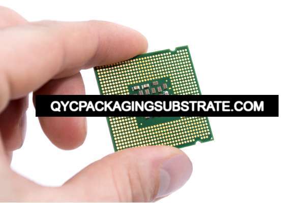
(MIS)Molded Interconnect Substrate Supplier, we mainly produce ultra-small bump pitch substrate, ultra-small trace and spacing bga packaging substrates from 2 layer to 22 layers.
Molded Interconnect Substrate (MIS), known as molded interconnect substrate in Chinese, is a technology that plays a key role in PCB design and manufacturing. It prints circuits on a three-dimensional plastic substrate to integrate circuit functions and structures. This article will delve into the definition, working principle and importance of MIS in modern electronic equipment, and analyze the key role of this technology in the electronics industry for readers.
What is MIS?
Molded Interconnect Substrate (MIS), or molded interconnect substrate, represents an advanced circuit board manufacturing technology. Its innovation lies in printing circuits directly on three-dimensional plastic substrates, thereby achieving the perfect integration of circuit function and structure. Through the clever use of injection molding and conductive fillers, MIS has brought major breakthroughs to the design and manufacturing of electronic devices.
Traditional PCB design usually relies on circuit layout on a two-dimensional plane, and the introduction of MIS technology makes circuit design no longer limited to plane space, but can be laid out in three-dimensional space, thereby achieving more complex and dense circuits. structure. By directly injecting conductive fillers on plastic substrates, MIS achieves free layout of conductive paths, greatly improving circuit integration and performance.
The core of MIS technology lies in the injection molding in its manufacturing process. In this process, a plastic substrate is injected into a mold and shaped under high temperature and pressure, while being filled with conductive material to form a conductive path. This integrated manufacturing method not only simplifies the manufacturing process, but also greatly improves the reliability and stability of the circuit. In addition, MIS can also realize the design of multi-layer circuits, further improving the integration and performance of the circuit.
Overall, MIS technology brings great convenience and innovation to the design and manufacturing of electronic devices. By integrating circuit functions and structures, MIS not only improves circuit integration and performance, but also brings more possibilities and flexibility to the design of electronic devices. In the future, with the continuous development and improvement of MIS technology, I believe it will play an increasingly important role in the electronics industry, injecting new impetus into innovation and progress.
How to Design a PCB with MIS?
Designing PCBs using Molded Interconnect Substrate (MIS) requires specific process and software support. MIS technology prints circuits on three-dimensional plastic substrates to integrate circuit functions and structures. Therefore, many factors need to be considered during the design stage to ensure circuit performance and reliability.
First, designers need to take into account the special structure and manufacturing process of MIS when doing circuit layout. Since the circuits will be printed directly on the plastic substrate, overly complex or dense designs need to be avoided during layout to ensure the feasibility of the molding process. Reasonable layout can not only improve the reliability of the circuit, but also reduce manufacturing costs.
(MIS)Molded Interconnect Substrate
Secondly, material selection is crucial to MIS design. Designers need to choose plastic materials suitable for the MIS process and ensure they have good thermal stability and mechanical strength. At the same time, the selection of conductive fillers also needs to take into account its compatibility with the plastic substrate and its conductive properties to ensure that the conductive path of the circuit is unobstructed.
When choosing software tools, designers should give priority to professional software that can support MIS design. These software usually have the specific functions and process support required for MIS design, and can help designers realize complex circuit layout and optimization, while providing simulation and simulation functions to verify the feasibility and performance of the design.
In general, designing PCBs using MIS requires designers to have in-depth technical understanding and process knowledge, as well as the ability to skillfully use professional software. By comprehensively considering factors such as circuit layout, material selection, and software support, designers can achieve high-performance, high-reliability MIS PCB design and provide technical support for performance improvement and innovation of electronic equipment.
What is the (MIS)Molded Interconnect Substrate Fabrication Process?
The manufacturing process of MIS (Molded Interconnect Substrate) is a complex and precise process, involving multiple key steps, including material preparation, molding process, conductive filler and surface treatment. Compared with the traditional printed circuit board (PCB) manufacturing process, the manufacturing process of MIS is more complex because it requires the realization of complex circuit structures on a three-dimensional plastic substrate.
First, the first step in manufacturing MIS is material preparation. This includes selecting the appropriate plastic substrate material as well as conductive fillers. Plastic substrates usually use high-performance engineering plastics with good thermal stability and mechanical strength to ensure the stability and reliability of the final product. Conductive fillers are key materials for forming circuit patterns on plastic substrates and need to have good conductive properties and adhesive properties.
Secondly, the molding process is one of the key steps in the MIS manufacturing process. The molding process usually uses injection molding technology to integrate a plastic substrate and conductive filler. During the molding process, molding temperature, pressure and time need to be precisely controlled to ensure the dimensional accuracy and surface quality of the final product.
The selection and application of conductive fillers are also key links in the MIS manufacturing process. Conductive fillers need to form a reliable conductive path after molding and be able to connect well with other components. Manufacturers need to select appropriate conductive fillers based on the requirements of the circuit design and ensure their even distribution and precise coating during the molding process.
Finally, surface treatment is the final process step in the MIS manufacturing process. Surface treatments often include metallization and surface coatings to improve the electrical conductivity and corrosion resistance of the circuit. Metallization usually uses chemical gold or silver plating to form a conductive layer to improve the conductivity and reliability of the circuit. Surface coating can increase the corrosion resistance and environmental adaptability of the circuit and extend its service life.
In general, the manufacturing process of MIS involves multiple key steps and requires high-precision equipment and process control. By carefully designing and strictly executing each step, manufacturers can ensure the quality and performance of the final product to meet customer demands for high-performance electronic devices.
How to manufacturing a (MIS)Molded Interconnect Substrate?
Manufacturing PCBs for MIS requires specialized equipment and technical support. Compared with traditional double-sided or multi-layer PCB, the manufacturing process of MIS PCB is more complex and requires precision molding equipment and professional technology. During the molding process, manufacturers must consider a variety of factors to ensure the quality and performance of the final product.
First, the thermal expansion coefficient of the material needs to be considered during the molding process. Since MIS PCB usually uses plastic substrates, during the molding process, the thermal expansion coefficient of the material is crucial to the dimensional accuracy after molding. Manufacturers must accurately control molding temperature and pressure based on material characteristics and design requirements to ensure the dimensional stability of the final product.
Secondly, the molding temperature also needs to be considered during the molding process. Temperature control is critical to maintaining the conductive properties of the filler. High temperatures or uneven temperature distribution may cause the filler to sinter or degrade in conductive properties, affecting PCB performance and reliability. Therefore, manufacturers must use high-precision temperature control systems and adjust the molding temperature according to the characteristics and requirements of the filler.
In addition, the conductive properties of the filler are also one of the important factors to consider when manufacturing MIS PCB. The filler must have good electrical conductivity properties to ensure that the connection and transmission of the circuit function properly. Manufacturers must select appropriate filler materials and ensure good adhesion and compatibility with substrate materials to improve circuit reliability and stability.
Throughout the entire manufacturing process, manufacturers need to strictly control each step, including material preparation, molding process, filler injection, molding temperature and pressure control, and final quality inspection. Through strict quality control and process management, manufacturers can ensure that the final product meets customer requirements and standards and has excellent performance and reliability.
In short, manufacturing MIS PCB requires specialized equipment and technical support to ensure precise control of various parameters during the molding process and the quality and performance of the final product. Manufacturers must pay close attention to material selection and processing, molding temperature control, and filler conductive properties to ensure the production of high-quality MIS PCB products that meet customer needs.
How Much Does a PCB with MIS Cost?
Molded Interconnect Substrate (MIS), as an advanced PCB technology, plays a key role in improving the performance and integration of electronic devices. However, MIS does cost more than traditional PCBs. This is mainly because MIS involves a series of complex processes and materials, requiring a higher level of technology and sophisticated manufacturing equipment.
First, the cost of MIS is affected by material costs. Compared with traditional FR4 substrates, the molding materials and conductive fillers used in MIS are generally more expensive. These materials need to have excellent thermal stability, mechanical strength and electrical conductivity to ensure the reliability and stability of the PCB.
Secondly, the manufacturing process is also one of the important factors affecting the cost of MIS. Compared with traditional PCB manufacturing, the manufacturing process of MIS is more complex and requires higher craftsmanship and more sophisticated equipment. Processes such as injection molding, conductive filler injection, and surface treatment all require precise control, which increases manufacturing costs.
In addition, design complexity will also affect the cost of MIS. Since MIS can achieve more complex circuit design and higher integration, the design process may be more cumbersome, requiring more engineer participation and more design resource investment. These will increase the design cost, thereby indirectly affecting the price of the final product.
Finally, production scale is also one of the factors affecting MIS costs. Typically, MIS costs are higher for low-volume production because manufacturers need to spread fixed costs. In contrast, mass production can reduce unit costs because fixed costs can be spread over more products.
Although the cost of MIS is relatively high, its performance and integration are also higher. MIS can achieve more complex circuit design, higher density and better electrical performance, thus providing more possibilities for improving the performance of electronic devices. Therefore, despite the higher cost of MIS, investing in MIS technology may be a wise choice for some applications with higher performance requirements.
What Materials are MIS PCBs Made Of?
The manufacturing of Molded Interconnect Substrate (MIS) involves a variety of key materials that play a vital role in ensuring the reliability and stability of PCBs. The following is a detailed introduction to the main materials of MIS PCB:
The basis of MIS PCB is a plastic substrate, usually using high-performance plastics such as polyimide (PI) or polyamide (PA). These plastics have excellent thermal stability and mechanical strength, allowing them to remain stable under a wide range of environmental conditions. In addition, plastic substrates must have good chemical stability to ensure that corrosion or damage does not occur during manufacturing and use.
The conductive filler in MIS PCB is a key component to achieve circuit connection. Commonly used conductive fillers include silver paste, carbon nanotubes and copper fillers. These fillers must have good electrical conductivity to ensure the proper functioning of the circuit. In addition, the conductive filler needs to have good adhesion and stability to ensure a strong and long-lasting bond with the plastic substrate.
The surface coating is the outermost layer of the MIS PCB and is used to protect the circuit and provide surface connections. Common surface coating materials include gold, silver, tin and nickel. These materials not only have good electrical conductivity, but also have good corrosion resistance and wear resistance, which can effectively protect the circuit and ensure the reliability of the connection. In addition, surface coatings can provide an additional layer of protection against the effects of external environmental factors on the circuit.
These materials play an integral role in the manufacturing process of MIS PCB. They require precise material selection and processing to ensure excellent performance and reliability of the final product. By rationally selecting and using these materials, manufacturers can produce high-quality MIS PCBs suitable for various application scenarios, promoting the continuous development and innovation of electronic technology.
Who Manufactures PCBs with MIS?
As a manufacturer of MIS PCB, our company adheres to the concepts of technological innovation and quality priority to provide customers with high-performance, high-reliability MIS PCB solutions. We have advanced production equipment and an experienced technical team, dedicated to meeting our customers’ various needs for MIS PCBs.
Our technical team has extensive experience in PCB design and manufacturing and is familiar with various MIS manufacturing processes and technical specifications. We have advanced CAD/CAM software and simulation tools to provide customers with a full range of design support and technical consulting services.
We have advanced production equipment and automated production lines, capable of meeting large-scale production and customization needs. We focus on lean management and quality control of the production process to ensure that each MIS PCB can meet customer expectations.
Our company strictly implements the ISO quality management system, and all production processes undergo strict quality control and testing. We use advanced testing equipment and technical means to ensure that each MIS PCB can operate stably and reliably.
Our company is customer-centric, adhering to the principles of integrity, professionalism and efficiency, and provides customers with high-quality services and technical support. We maintain close communication with our customers, solve their problems and needs in a timely manner, and help them succeed in market competition.
We are committed to providing customers with customized MIS PCB solutions, designing and producing according to customers’ specific needs and application scenarios. Our flexible production capabilities and fast response speed can meet customer requirements for product performance, delivery cycle, etc.
As a MIS PCB manufacturer, we will continue to adhere to the concepts of technological innovation and quality first, continuously improve product quality and technical level, and provide customers with better products and services.
What are 5 qualities of a good customer service?
In the PCB manufacturing industry, providing excellent customer service is crucial. Good customer service not only builds long-term relationships, it also enhances a manufacturer’s reputation and competitive advantage. Here are five key metrics for measuring a manufacturer’s customer service quality:
Professionalism is the cornerstone of customer service. Manufacturers should have extensive industry knowledge and experience and be able to provide customers with accurate, professional advice and solutions. Whether it is technical support, design consultation or after-sales service, professionalism and professionalism should be reflected.
Prompt response is key to building good customer relationships. Manufacturers should keep communication channels open and respond to customer inquiries and questions in a timely manner. Whether it’s via email, phone or online chat, make sure customers receive prompt feedback and solutions.
Customer service should be personalized, providing customized services based on the customer’s specific needs and preferences. Manufacturers should have a deep understanding of customers’ business and product needs, actively listen to customer feedback, and adjust service plans based on customer feedback and needs.
Good customer service should be able to resolve customer issues and challenges in a timely and effective manner. Manufacturers should have the ability to quickly identify the root cause of problems, analyze solutions, and actively assist customers in solving problems to ensure that customers’ production lines are not affected.
Continuous improvement in customer service quality is key to maintaining competitive advantage. Manufacturers should constantly collect customer feedback and suggestions, analyze changing trends in customer needs, and continuously optimize and improve customer service processes and solutions to meet the changing needs of customers.
In the PCB manufacturing industry, high-quality customer service can not only improve customer satisfaction and loyalty, but also help manufacturers establish a good brand image, expand market share, and achieve sustainable development. Therefore, manufacturers should pay attention to customer service quality and continuously improve service levels to meet customer needs and expectations.
FAQ
What is MIS (Molded Interconnect Substrate)?
MIS is an advanced PCB manufacturing technology that integrates circuit functions and structures by printing circuits on three-dimensional plastic substrates. Its main feature is the use of injection molding and conductive fillers to tightly combine the circuit with the substrate, thereby improving the integration and performance of the PCB.
What is the difference between MIS PCB and traditional PCB?
There are obvious differences between MIS PCB and traditional PCB in manufacturing process and structure. MIS PCB uses molding technology to embed the circuit directly into the plastic substrate, while traditional PCB prints the circuit on a flat substrate. This enables MIS PCB to have higher integration, better performance and wider application scenarios.
What are the advantages of MIS PCB?
MIS PCB has many advantages over traditional PCB. First, MIS PCB has higher integration and smaller size because the circuit is directly embedded in the substrate. Secondly, MIS PCB can realize more complex circuit design and provide more diverse product choices. In addition, MIS PCB also has good thermal stability and mechanical strength, making it suitable for various harsh working environments.
What is the manufacturing cost of MIS PCB?
The manufacturing cost of MIS PCB is relatively high, mainly depending on factors such as material cost, manufacturing process and design complexity. Compared with traditional PCBs, MIS PCBs require higher-precision equipment and process control, so manufacturing costs will increase. However, with the continuous advancement of technology and the growth of market demand, the cost of MIS PCB is gradually decreasing.
How to choose a suitable MIS PCB manufacturer?
There are several factors to consider when choosing the right MIS PCB manufacturer. First of all, the manufacturer’s technical strength and production capacity are key factors, and manufacturers with rich experience and advanced equipment should be selected. Secondly, the manufacturer’s quality control level and customer service capabilities are also crucial. You should choose a manufacturer that can provide high-quality products and respond in a timely manner.