 Professional Flip-Chip Packaging Substrate Supplier

Multi-cavity PCB | RF Cavity PCB manufacturing. Open Multi cavity PCBs. To use the High-frequency materials, high-speed materials, or other kinds of materials, we can produce the multi-cavity PCBs from 4 layer to 30 layers.
In modern electronics, the magic often hides in invisible places – on the printed circuit board (PCB). These compact marvels are the building blocks of our devices, weaving the symphony of electrical signals that drive our world. Today, we’ll delve into the fascinating world of multi-cavity PCB manufacturing, revealing its complexities and unlocking its potential.
What is a multi-cavity PCB?
In the field of modern electronics, multi-cavity PCB is an innovative circuit board design designed to meet the needs of increasingly complex electronic devices. A traditional single-cavity PCB (Printed Circuit Board) mounts all components on a single plane, while a multi-cavity PCB divides the circuit board into multiple cavities or areas, each of which can accommodate independent electronic components or subsystem. The core of this design concept is to create multiple isolated spaces on a single circuit board, so that different functional modules can work independently of each other and are physically separated from each other, thus improving the flexibility and performance of the overall system.
The design of multi-cavity PCBs is often affected by factors such as product complexity, space constraints, and performance requirements. By segmenting the board into multiple cavities, designers can better manage routing, reduce interference, and optimize the placement of electronic components to maximize board performance and reliability. This design method is particularly suitable for electronic equipment with high density, high frequency, high power and complex functions, such as communication equipment, medical instruments, aerospace equipment, etc.
By employing multi-cavity PCB designs, engineers can achieve higher levels of integration and more optimized system designs. For example, a smart device with sensors, processors and communication modules could place each functional module in a separate chamber to ensure electromagnetic compatibility with each other and simplify maintenance and repair of the system. In addition, multi-cavity PCB also provides more possibilities for modular design and product upgrades, because different functional modules can be changed and updated relatively independently.
Overall, multi-cavity PCBs represent an important advancement in electronics design and manufacturing, providing engineers with more flexible and efficient solutions. With the continuous advancement and innovation of technology, multi-cavity PCB will continue to play a key role in promoting the development and evolution of electronic products.
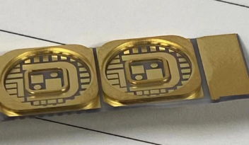
Multi-cavity PCB
How about the design of multi-cavity PCB?
Designing a multi-cavity PCB is a comprehensive process that requires several key steps to achieve. Here are the key steps for designing a multi-cavity PCB:
Before designing a multi-cavity PCB, the entire system architecture needs to be designed first. This includes determining the functional requirements of the system, how various subsystems communicate with each other, and how different modules are connected. Through system architecture design, the role and functional positioning of each cavity in the entire system can be clarified.
According to the system architecture design, the entire PCB board is divided into multiple cavities. Each cavity can house one or more electronic components or subsystems. Cavity partitioning needs to take into account the interaction between electronic components and minimize electromagnetic interference.
After determining the cavity divisions, component layout needs to be performed for each cavity. This involves placement and orientation of electronic components to maximize routing efficiency and signal integrity on the PCB. During the layout process, it is necessary to consider the interconnection between components, heat dissipation requirements, and rational use of space.
After completing the component layout, the next step is the design of signal routing. Signal routing refers to the process of connecting signal lines between various electronic components. In multi-cavity PCB design, special attention needs to be paid to signal transmission between different cavities to ensure matching and electromagnetic compatibility of high-speed signal lines.
Another important design consideration is power management. Multi-cavity PCBs usually require different power supplies for different cavities, so it is necessary to design an effective power distribution scheme and take measures to reduce power supply noise and fluctuations.
After the design is completed, integrity verification needs to be performed. This includes electrical rule checks (DRC) and signal integrity analysis (SI) to ensure the design meets specifications and is functioning properly. In addition, electromagnetic compatibility testing (EMC) and thermal analysis are also required to ensure the stability and reliability of the design.
Finally, simulation tools can be used to simulate and optimize the design. Through simulation analysis, the performance of different design options can be evaluated, and the necessary adjustments and optimizations can be made to the design to ensure that the final multi-cavity PCB design meets performance and reliability requirements.
To sum up, designing multi-cavity PCB is a complex and meticulous process, which requires designers to have solid electronic design knowledge and rich experience to ensure the accuracy and reliability of the design.
What is the process of manufacturing a multi-cavity PCB?
Manufacturing multi-cavity PCBs is a complex and delicate process involving multiple critical steps, each of which is crucial. The following are the key steps in the multi-cavity PCB manufacturing process:
Design Verification: Before manufacturing a multi-cavity PCB, the design first needs to be verified. This includes ensuring that the design meets specifications and requirements, checking that circuit connections are correct, and assessing the suitability of the layout. Through design verification, errors and unnecessary costs in the manufacturing process can be minimized.
Material Preparation: The first step in manufacturing a multi-cavity PCB is to prepare the required materials. This typically involves selecting an appropriate substrate material, such as FR-4 (fiberglass reinforced epoxy), and determining the correct thickness and size of copper foil. Choosing high-quality materials is critical to ensuring the performance of the final PCB.
Layer Stacking: Multi-cavity PCB is usually composed of multiple layers, each layer carrying specific circuit components or signals. In the layer stacking stage, these layers are stacked together according to the design specifications to form an overall panel structure.
Pattern Drawing: The next step is the process of drawing circuit graphics on the board. Through chemical etching or photolithography, patterns are formed on the copper foil layer to form wires and holes for circuit connections.
Chemical Etching: After drawing the pattern, the board is placed in a chemical etching solution to remove the unprotected portion of the copper foil, leaving the desired circuit pattern. This step ensures the accuracy and consistency of the circuit.
Drilling: Next is the process of drilling holes on the PCB to install components and achieve circuit connections. Through high-precision drilling equipment, holes are precisely drilled on the PCB to ensure the accuracy and stability of component installation.
Surface Finishing: PCB surface treatment is to improve the corrosion resistance and welding performance of PCB. This may include treatments such as gold plating, tin spraying, lead spraying, etc. to protect the PCB surface and provide good solder contact.
Inspection and Testing: Finally, the final step in the manufacturing process is inspection and testing of the PCB. Ensure PCBs meet design specifications and achieve expected performance levels through methods such as visual inspection, automated optical inspection, and electrical testing.
To sum up, manufacturing multi-cavity PCB is a comprehensive process that requires precise design, sophisticated equipment and strict quality control. Each step plays a vital role in the quality and performance of the final product, and a sound manufacturing process is key to ensuring that the PCB can operate stably and reliably in a variety of applications.
How much does a multi-cavity PCB cost?
The manufacturing cost of multi-cavity PCB is a complex calculation process involving multiple factors. First, you need to consider the costs of the design phase, including software licensing fees, design engineer salaries, and the time required to design. As design complexity increases, design costs tend to increase accordingly.
Secondly, material cost is one of the key factors that determines the manufacturing cost of multi-cavity PCB. This includes the cost of substrate material (such as FR-4), copper thickness, and additional materials such as pads and solder paste. The choice of different materials can have a direct impact on costs, with higher quality materials generally resulting in higher costs.
The process and labor costs in the manufacturing process are also an important part of the manufacturing cost. This includes depreciation expenses for equipment such as CNC machine tools, etching equipment, drilling machines and assembly lines, as well as operator wages and training costs. Complex multi-cavity designs may require more processing steps and labor input, resulting in a corresponding increase in manufacturing costs.
Another factor that affects multi-cavity PCB manufacturing costs is production scale and lead time. Typically, high-volume production reduces unit costs because fixed costs can be spread over more boards. Additionally, shorter lead times often result in rush manufacturing, which can increase production costs.
Finally, there are additional costs to consider, such as shipping charges, taxes, and any possible additional expenses for corrections and remanufacturing. Although these costs may account for a relatively small proportion of the entire production process, they also need to be included in the consideration of manufacturing costs.
To sum up, the manufacturing cost of multi-cavity PCB is a complex process that takes into account many factors, among which design complexity, material selection, manufacturing process and production scale will directly affect the final cost. Therefore, when estimating multi-cavity PCB manufacturing costs, various factors need to be considered comprehensively to ensure accurate estimation and control of manufacturing costs.
What materials are multi-cavity PCBs made of?
Multi-cavity PCB (Printed Circuit Board) is a core component of modern electronic equipment, and its material selection is crucial. In multi-cavity PCB manufacturing, a range of high-quality materials are typically used to ensure the performance, reliability, and durability of the board.
The substrate of multi-cavity PCB usually uses fiberglass reinforced epoxy resin (FR-4) as the main material. FR-4 substrate has excellent mechanical strength and heat resistance and is suitable for applications under various environmental conditions. In addition, there are some high-performance substrate materials, such as polyimide (PI) and polytetrafluoroethylene (PTFE), which can be used in special applications.
The conductive layer of multi-cavity PCBs usually uses copper, whose excellent conductivity and processability make it an ideal choice. The conductive layer is precision processed and etched to form structures such as wires and pads for circuit connections.
In addition to conductive layers, multi-cavity PCBs also contain insulating layers to isolate different levels of circuitry. Common insulation materials include etched fiberglass cloth, polyimide film, etc., which have good insulation properties and high temperature resistance.
As the connection medium for electronic components, the pads on multi-cavity PCBs usually use tin-lead alloy or lead-free solder. These materials have good soldering properties and reliability, ensuring a solid connection between electronic components and PCBs.
Multi-cavity PCBs are usually covered with a special cladding layer to protect the circuit structure from the external environment. Common coating materials include epoxy resin, polyimide resin, etc., which have good corrosion resistance and insulation properties.
For some special application areas, such as high frequency, high speed, high density, etc., special materials may be needed to meet performance requirements. For example, polytetrafluoroethylene (PTFE) substrates can be used in high-frequency circuit designs and have excellent dielectric properties and signal transmission characteristics.
To sum up, multi-cavity PCB is usually composed of various materials such as substrate material, conductive layer, insulating layer, pad material, cladding material and so on. These materials play a key role in multi-cavity PCB manufacturing, determining the board’s performance and reliability. With the continuous advancement of technology, new materials and processes are constantly emerging in the field of multi-cavity PCB manufacturing, providing a broader space for the development of electronic equipment.
Who makes multi-cavity PCBs?
In the modern electronics industry, the process of manufacturing multi-cavity PCBs is a task that requires highly specialized knowledge and skills. So, who makes multi-cavity PCBs? In many cases, the manufacturing of multi-cavity PCBs is done by professional PCB manufacturers. For some companies, having their own PCB manufacturing facilities may be more ideal.
At our company, we are aware of the growing demand for multi-cavity PCBs and the importance of providing high-quality PCBs. Therefore, we have established our own PCB manufacturing facilities to meet the needs of our customers. Our PCB manufacturing factory has advanced equipment and technology, capable of producing various types of PCBs, including single-layer, double-layer and multi-layer PCBs, as well as complex multi-cavity PCBs.
At our PCB manufacturing factory, we have gathered an experienced team with professional knowledge and skills in the field of PCB manufacturing. Our engineers and technicians work closely together to ensure that every manufacturing process meets the highest standards and meets our customers’ needs.
In addition to having advanced equipment and a professional team, we also focus on quality management and customer service. We strictly control every production stage, from raw material procurement to final delivery, to ensure product quality and reliability. At the same time, we are committed to establishing good cooperative relationships with customers, understanding their needs and providing customized solutions.
As a PCB manufacturer, we not only provide products, but also a solution partner. We are always committed to providing the best PCB manufacturing services to our customers to meet their ever-changing needs. Therefore, whether it is a simple single-layer PCB or a complex multi-cavity PCB, we are able to provide customers with satisfactory solutions.
In short, multi-cavity PCBs are manufactured by PCB manufacturers with extensive experience and expertise. And at our company, we provide customers with high-quality, reliable multi-cavity PCB manufacturing services by having our own PCB manufacturing facilities and focusing on quality management and customer service.
How important is it to provide quality service?
In multi-cavity PCB manufacturing, providing quality service is crucial. First, quality service can ensure that customers’ needs are fully met, thereby enhancing customer satisfaction and establishing good business relationships. In multi-cavity PCB manufacturing, customers often have specific design requirements and technical needs, and providing quality service can ensure that these requirements are understood and met in a timely manner. By working closely with customers, manufacturers can better understand their needs and provide ongoing support and feedback during the design, manufacturing and delivery processes.
Secondly, quality service can help manufacturers build a good reputation and brand image. In a competitive market, a good reputation is key for manufacturers to attract new customers and retain existing ones. By providing high-quality products and services, as well as professional and thoughtful customer support, manufacturers can win the trust and recognition of customers, thereby establishing a reliable and trustworthy brand image.
In addition, quality service can also improve production efficiency and product quality. By establishing a close working relationship with customers, manufacturers can better understand their needs and expectations, thereby arranging production plans and resource allocation more effectively. In addition, timely communication and feedback can also help manufacturers discover and solve potential problems in time, thereby ensuring product quality and delivery time.
Finally, high-quality services can promote the continued development and innovation of the industry. By working with customers, manufacturers can continuously improve product design and manufacturing processes and promote the continuous advancement of industry technology. In addition, by sharing the latest industry trends and technological developments with customers, manufacturers can inspire customers’ sense of innovation and jointly drive the industry forward.
To sum up, in multi-cavity PCB manufacturing, providing high-quality services not only helps meet customer needs and establish a good brand image, but also improves production efficiency and product quality, and promotes the sustainable development and innovation of the industry. Therefore, manufacturers should always prioritize providing quality services and place customer satisfaction at the forefront.
Frequently Asked Questions
What are the advantages of Multi-Cavity PCBs over traditional single-cavity designs?
Multi-Cavity PCBs offer several advantages over traditional single-cavity designs. Firstly, they allow for increased space efficiency by accommodating multiple components within a single board, making them ideal for compact electronic devices where space is at a premium. Additionally, Multi-Cavity PCBs offer enhanced functionality by enabling the integration of diverse subsystems, such as power management, signal processing, and communication modules, within a unified platform. Furthermore, Multi-Cavity PCBs streamline the assembly process by reducing the number of separate boards and interconnections required, thereby simplifying production and improving overall reliability.
How long does it take to manufacture Multi-Cavity PCBs?
The manufacturing lead time for Multi-Cavity PCBs varies depending on several factors, including complexity, volume, and the capabilities of the chosen manufacturer. Typically, the lead time ranges from a few days to several weeks. Simple designs with low volumes may be produced Relatively quickly, while complex designs or large production runs may require additional time for fabrication, assembly, and quality assurance processes.
Are there any environmental considerations in Multi-Cavity PCB manufacturing?
Yes, environmental considerations play an important role in Multi-Cavity PCB manufacturing. Many manufacturers prioritize eco-friendly practices to minimize environmental impact and promote sustainability throughout the production process. This includes using lead-free soldering materials to reduce hazardous waste, implementing energy- efficient manufacturing techniques to minimize resource consumption, and employing waste recycling programs to responsibly manage by-products and scrap materials. By adopting these environmentally conscious practices, Multi-Cavity PCB manufacturers can contribute to a more sustainable and eco-friendly electronics industry.
What are the key factors influencing the cost of Multi-Cavity PCBs?
The cost of Multi-Cavity PCBs is influenced by several key factors, including design complexity, board size, material selection, manufacturing volume, and additional features or special requirements. Complex designs with densely populated components and intricate routing patterns typically require more advanced fabrication processes and may incur higher manufacturing costs. Similarly, larger boards with multiple cavities or layers may require additional material and processing resources, resulting in increased production expenses. Additionally, factors such as expedited lead times, specialized materials, and custom specifications can also impact the overall cost of Multi-Cavity PCBs. By carefully considering these factors and working closely with the manufacturer, customers can optimize their designs to meet budgetary constraints without compromising quality or performance.