 Professional Flip-Chip Packaging Substrate Supplier

Multi cavity PCB manufacturing. the Package Substrate made with Multi cavity. Or open cavity on PCB boards. Our company has made many this types Multi cavity PCBs with High TG base materials or High-speed and high frequency materials.
In the electronics world, printed circuit boards (PCBs) are the backbone of countless devices, enabling connectivity and functionality. As technology advances, the demand for PCBs with improved performance, efficiency and compactness continues to grow. To meet this evolving need, multi-cavity PCB manufacturing processes have emerged as a significant solution.
What is a multi-cavity PCB?
Multi-cavity PCB (Printed Circuit Board) is an advanced electronic component that integrates multiple circuit cavities on a single circuit board. This design has many unique features that make it a key component in modern electronic devices.
In traditional single-chamber PCB designs, individual electronic components must be arranged in the same space, which may lead to problems such as cluttered wiring, signal interference, and insufficient heat dissipation. However, the emergence of multi-cavity PCBs solves these challenges, providing circuit designers with greater flexibility and performance advantages.
First of all, one of the biggest advantages of multi-cavity PCB is the maximization of space utilization. By integrating multiple circuit chambers onto a single board, designers can use space more efficiently, resulting in more compact, lighter device designs. This is especially important for applications that require compact size, such as mobile devices, embedded systems, and smart wearable devices.
Secondly, multi-cavity PCB design helps reduce signal interference. Each circuit chamber can be independently designed and optimized to minimize signal interference between electronic components. This isolation design can significantly improve system stability and performance, especially in high-frequency or high-speed applications.
Additionally, multi-cavity PCBs offer more flexible design options. Designers can allocate electronic components with different functions into different chambers based on specific application requirements to achieve customized solutions. This flexibility makes multi-cavity PCBs suitable for a variety of different application scenarios, from consumer electronics to industrial control systems.
Overall, the emergence of multi-cavity PCBs brings new possibilities and challenges to electronic designers. By integrating multiple circuit cavities onto a single board, multi-cavity PCBs achieve a balance of space optimization, signal isolation and design flexibility, providing important support for the performance improvement and innovative development of modern electronic devices.
How to design a multi-cavity PCB?
Designing multi-cavity PCBs involves a range of techniques and tools to ensure efficient layout of electronic components and minimal signal interference. The key steps and considerations required to design a multi-cavity PCB are detailed below:
First of all, designing multi-cavity PCB requires proficiency in circuit design software, such as Altium Designer, Cadence Allegro, etc. These software provide a wealth of tools and functions for drawing circuit diagrams, laying out components, performing signal routing, and more. Design engineers need to be familiar with the operating interfaces and functions of these software in order to effectively carry out design work.
Secondly, component layout and placement need to be considered when designing a multi-cavity PCB. Signal interference and crosstalk can be minimized through proper component placement. Design engineers need to reasonably arrange the positions of various components based on circuit function and performance requirements to avoid mutual interference between components.
In addition, designing multi-cavity PCBs also requires signal routing planning and optimization. The quality of signal routing directly affects the performance and stability of the circuit. Design engineers need to choose appropriate signal routing methods to avoid signal crossover and interference and ensure signal transmission quality.
When designing multi-cavity PCBs, factors such as thermal management and electromagnetic compatibility also need to be considered. Reasonable thermal management design can ensure the stable operating temperature of circuit components and improve the reliability and life of the circuit. Good electromagnetic compatibility design can reduce electromagnetic interference and ensure the normal operation of the circuit.
In short, designing multi-cavity PCB requires design engineers to have rich experience and professional knowledge, as well as the ability to skillfully use circuit design software and tools. Through reasonable component layout, optimized signal routing and good thermal management design, the performance and stability of multi-cavity PCB can be ensured to be optimal.
What are the advantages of multi-cavity PCB manufacturing?
In the field of modern electronics, multi-cavity PCB manufacturing, as an innovative design solution, brings many significant advantages, making it an increasingly popular choice. Here are the advantages of multi-cavity PCB manufacturing over traditional designs and the performance improvements it can provide:
The traditional single-cavity PCB design has limitations in space utilization, while the multi-cavity PCB effectively utilizes the board surface by integrating multiple circuit chambers into one board, making the overall device size smaller and suitable for applications with higher space requirements. Harsh application scenarios.
In multi-cavity PCB designs, signal paths can be better controlled and interference between different signals can be reduced. Through careful planning and layout, signal crossover between various chambers can be minimized, thereby improving the stability and reliability of the overall circuit.
The multi-cavity PCB design can better separate different functional modules and separate the heat generation area from the heat dissipation area, thereby managing and dispersing heat more effectively. This helps prevent local overheating and improves equipment efficiency and longevity.
Multi-cavity PCB design allows engineers to more flexibly arrange and organize various functional modules and components, making the design more customizable and flexible. This flexibility enables the design to better meet the needs of different application scenarios and improves the performance and adaptability of the overall system.
The advantages of multi-cavity PCB design directly lead to improved overall performance. By reducing signal interference, optimizing thermal management, and improving space utilization, multi-cavity PCBs can achieve more stable, reliable, and efficient circuit designs, thereby providing users with better product experience and performance.
In summary, multi-cavity PCB manufacturing has significant advantages in modern electronic design, not only improving the performance and stability of circuits, but also meeting the needs for space, thermal management and flexibility. With the continuous advancement of technology and the continuous expansion of application scenarios, multi-cavity PCB manufacturing will continue to play an important role in promoting the progress and development of electronic equipment.
What is the manufacturing process of multi-cavity PCB?
The manufacturing process of multi-cavity PCB is a complex and precise process designed to ensure accuracy and quality at every step to meet customer needs and ensure the performance and reliability of the final product.
First, the process of manufacturing a multi-cavity PCB begins with the preparation of design files. Engineers use professional PCB design software to convert the circuit diagrams provided by customers into specific design files to ensure that the layout and connection of each electronic component on the board comply with the design specifications.
Next is the preparation of raw materials. Choose high-quality substrate materials, such as FR-4 (fiberglass reinforced epoxy resin board) or other special materials to ensure the stability and durability of the PCB. The substrate is then surface-prepared for subsequent printing and etching, either through chemical treatment or mechanical processing.
This is followed by printed wiring and etching. By transferring the design file to the substrate, and using photolithography technology and chemical etching, the circuit pattern is printed onto the surface of the substrate and the unnecessary parts are etched away to form the required lines and connections.
After the wiring and connections are completed, drilling and plating are performed. A high-precision CNC drilling machine is used to drill the connection points on the PCB board for mounting electronic components. Then, metallization is applied to the drilled surface to ensure the reliability and conductivity of the connection.
The next step is surface preparation and coating. Coat the PCB surface with protective anti-corrosion and soldering materials to enhance the durability and stability of the PCB and prepare it for subsequent component installation.
Finally comes component installation and soldering. Electronic components are accurately mounted on the PCB through automated component mounting equipment, and the components and PCB are soldered together using wave soldering or surface mount technology to form a complete circuit.
Strict quality control is crucial throughout the entire manufacturing process. By using advanced inspection equipment and technology, each step is strictly inspected and tested to ensure manufacturing accuracy and quality. In addition, communication and feedback with customers are also key factors in ensuring that the final product meets customer requirements.
To sum up, the manufacturing process of multi-cavity PCB involves multiple complex steps and technologies designed to ensure the quality and performance of the final product, meet customer needs and promote the development of the electronics industry.
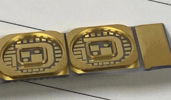
Multi cavity PCB
What materials are used in multi-cavity PCBs?
When manufacturing multi-cavity PCBs, selecting the appropriate materials is critical as they directly affect the performance, reliability and cost of the PCB. Here are some commonly used multi-cavity PCB materials:
FR-4: This is one of the most commonly used substrate materials and has good mechanical strength and heat resistance, making it suitable for most applications.
High-frequency materials: For high-frequency applications, such as communications equipment and radar systems, materials with lower losses and higher dielectric constants are required, such as PTFE (polytetrafluoroethylene) and RF-35.
Copper foil: Copper-clad material used on the surface of PCB to provide good conductivity and solderability.
Silver Materials: For applications requiring higher conductivity, silver-coated materials are available.
Polyimide (PI): Substrate material for flexible PCBs with excellent high temperature resistance and chemical resistance.
FR-4 substrate: Substrate for rigid PCB, providing stable structural support.
Solder film: used to cover the PCB welding area and protect the PCB surface from contamination and damage during the welding process.
Protective paint: used to cover the PCB surface to provide moisture-proof, anti-corrosion and insulation functions.
Epoxy resin: used to fill holes and gaps in PCB to enhance the mechanical strength and stability of PCB.
Polyamide: has good fluidity and adhesion, suitable for filling small pores and small voids.
Selecting the appropriate material depends on several factors, including application environment, budget constraints, performance requirements and manufacturing processes. Therefore, PCB design engineers need to carefully evaluate the advantages and disadvantages of each material and select based on specific needs. At the same time, by establishing a good cooperative relationship with material suppliers, you can obtain more technical support and resources to ensure the successful implementation of PCB manufacturing.
Who are the leading multi-cavity PCB manufacturers?
In the field of multi-cavity PCB manufacturing, it is crucial to choose a reliable and technologically leading supplier. The company is proud to be a leader in this field, not only adhering to high standards of quality control but also maintaining a constant commitment to innovation and customer satisfaction.
As a leading multi-cavity PCB manufacturer, our company has extensive technical expertise and experience. Our engineering team is proficient in a variety of design software and tools and can flexibly handle a variety of complex design needs. Whether it is layout optimization or signal transmission optimization, we can provide professional guidance and solutions. In addition, we continue to invest in technological innovation and R&D to ensure that our products are at the forefront of the industry.
Quality is one of our company’s core values. We strictly implement the ISO quality management system and all products undergo strict quality control and testing procedures to ensure that they meet our customers’ high standard requirements. We use advanced production equipment and processes to ensure product consistency and reliability.
We know that our customers’ needs are diverse, so we provide flexible customized services to meet the specific needs of different customers. Whether from design to production or after-sales service, we maintain close communication with our customers to ensure that their needs are fully understood and met. Our customer service team is always customer-focused and dedicated to providing support and assistance to customers.
As a responsible company, we are committed to sustainable development and environmental responsibility. We use environmentally friendly materials and production processes to reduce our impact on the environment. At the same time, we strictly abide by industry norms and laws and regulations to ensure that all products comply with relevant standards and requirements.
As a leading multi-cavity PCB manufacturer, we continue to provide customers with high-performance, reliable solutions based on excellent quality, technological innovation, customer orientation and sustainable development. We look forward to cooperating with you to jointly promote the development and progress of electronic technology.
How to provide excellent customer service?
In the process of becoming a great multi-cavity PCB manufacturer, providing excellent customer service is crucial. Here are the key attributes and practices to ensure customer satisfaction:
Effective communication is the basis for building good customer relationships. Promptly responding to customer inquiries, needs and feedback and maintaining transparent and open communication channels can enhance customer trust and reduce misunderstandings.
As a multi-cavity PCB manufacturer, it is crucial to have solid technical expertise. Able to provide professional suggestions and solutions to help customers solve technical problems and enhance customer trust and satisfaction in the company.
Understand customer needs and provide personalized and customized services based on their specific requirements. From design to production, flexible adjustments and optimizations are made according to customer needs to ensure that products can fully meet customer expectations.
Ensure product quality and delivery on time. Through strict quality control and management processes, we ensure that the quality of each batch of products is stable and reliable and delivered to customers on time, thereby enhancing customer confidence and satisfaction.
Provide comprehensive after-sales support and service. After product delivery, we continue to keep in touch with customers and provide services such as technical support, repairs, and updates to ensure customers have a smooth experience when using the product.
Build a culture of continuous improvement and proactively seek customer feedback. Through regular customer satisfaction surveys and feedback mechanisms, we collect customer opinions and suggestions and continuously optimize products and services to meet the changing needs of customers.
Not just content with one-time transactions, but actively building long-term relationships. By building trust and partnership with customers, we grow and develop together to achieve a win-win situation.
In practice, an excellent multi-cavity PCB manufacturer will regard customer service as the core strategy of corporate development, and continuously invest resources and energy to improve customer satisfaction and loyalty. Through the implementation of the above characteristics and practices, these manufacturers can win the trust and respect of their customers and stand out in the market competition.
FAQs
What are the primary applications of Multi-Cavity PCBs?
Multi-Cavity PCBs find extensive applications across diverse industries due to their versatility and space-saving advantages. They are commonly used in telecommunications for networking equipment, automotive electronics for control systems and sensors, aerospace for avionics and navigation systems, consumer electronics for compact devices such as smartphones and tablets, and medical devices for diagnostic equipment and monitoring devices. The ability to integrate multiple functions within a single board makes Multi-Cavity PCBs indispensable in modern electronic systems.
How does Multi-Cavity PCB manufacturing differ from traditional PCB fabrication?
Traditional PCB fabrication typically involves the creation of single-layer or double-layer boards with a single circuit layer. In contrast, Multi-Cavity PCB manufacturing integrates multiple circuit cavities within a single board, enabling higher component density, improved signal integrity, and enhanced functionality in a compact form factor. The design and manufacturing processes for Multi-Cavity PCBs are more complex, requiring specialized expertise and advanced equipment to achieve precise alignment and interconnection of multiple cavities.
What factors should be considered when designing Multi-Cavity PCBs?
Designing Multi-Cavity PCBs requires careful consideration of several factors to ensure optimal performance and reliability. Key considerations include component placement to minimize signal interference, routing paths to maintain signal integrity and impedance control, thermal management to dissipate heat efficiently, compatibility with assembly processes to facilitate manufacturing, and adherence to industry standards and regulations. Additionally, designers must anticipate future scalability and customization requirements to accommodate evolving needs.
What are the advantages of choosing Multi-Cavity PCBs over traditional PCBs?
Multi-Cavity PCBs offer several advantages over traditional PCBs, including space optimization, enhanced performance, cost efficiency, customization options, and scalability. By consolidating multiple functions into a single board, Multi-Cavity PCBs reduce overall system footprint, minimize interconnect complexity, and improve signal integrity. This results in higher reliability, lower assembly costs, and faster time-to-market for electronic products. Additionally, Multi-Cavity PCBs provide greater flexibility for accommodating diverse application requirements and evolving technology trends.
How can customers ensure the quality and reliability of Multi-Cavity PCBs?
Customers can ensure the quality and reliability of Multi-Cavity PCBs by partnering with reputable manufacturers that adhere to stringent quality control standards and certifications. It is essential to verify the manufacturer’s track record, industry reputation, and adherence to regulatory requirements. Additionally, customers should collaborate closely with manufacturers during the design and testing phases to address any potential issues and optimize performance. Regular communication, transparency, and collaboration are key to ensuring a successful partnership and delivering high-quality Multi-Cavity PCBs that meet or exceed customer expectations.