 Professional Flip-Chip Packaging Substrate Supplier

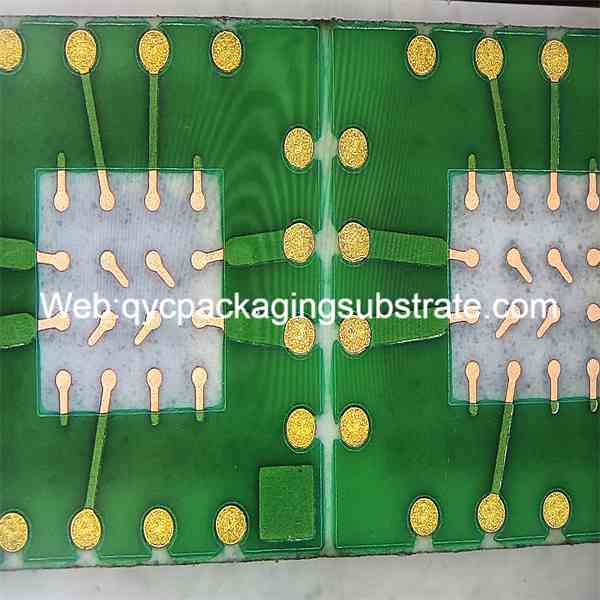
Package substrate structure and package substrate manufacturer. We use advanced Msap and Sap technology, High multilayer interconnection substrates from 2 to 20 layers.
In the booming development of the electronics industry, Package Substrate, as one of the key components, plays a pivotal role in connecting chips and circuit boards. In short, Package Substrate is a key electronic packaging technology used to connect chips to system-level packages for electrical connections, thermal management, and structural support.
The core of this packaging technology is to provide a reliable platform so that the chip can perform its functions in practical applications. It is responsible for transmitting signals, power and heat, and plays a vital role in the performance and stability of electronic equipment. Therefore, a deep understanding of the different structures and properties of Package Substrate is crucial to advance the development of electronic technology.
It is within the diversity of Package Substrate that we find a variety of innovative designs and structures. This article will delve into different Package Substrate structures, including the traditional Chip-on-Substrate (CoS) and Chip-in-Substrate (CiS) structures, as well as the more advanced Fan-Out Wafer/Panel Level Package (FoWLP) structure, Rigid -Flex architecture, as well as the emerging Embedded Component Package (ECP) architecture and Silicon Interposer architecture.
Through the analysis of these structures, we will reveal their applications and advantages in electronic devices, providing engineers, designers, and decision-makers with insights into selecting appropriate Package Substrate structures in different application scenarios. Let us dig deeper into the mysteries of these packaging substrates and promote the electronics industry to take more solid steps in technological innovation and sustainable development.
Package substrate structure
Traditional Package Substrate structure
In the design world of Package Substrate, traditional structures play a key role, including Chip-on-Substrate (CoS) and Chip-in-Substrate (CiS) structures. These classic structures play an irreplaceable role in electronic packaging. The following is a detailed analysis:
Explanation of basic principles: The CoS structure is a design in which the chip is directly packaged on the surface of the substrate. The key to this structure is to directly connect the chip to the substrate to achieve a high degree of compactness and good electrical performance.
Application in packaging: CoS structures are widely used in a variety of electronic devices, especially in scenarios that require high space efficiency and heat dissipation performance. Microchips and sensors often use CoS structures to increase integration and reduce package size.
Chip-in-Substrate (CiS) structure
Introduction to design concept: CiS structure is a structure in which a chip is embedded in a substrate. Unlike CoS, CiS achieves a higher degree of assembly flexibility and protection by nesting chips within a substrate.
Typical applications in electronic equipment: CiS structures are commonly found in scenarios with relatively loose packaging space requirements, such as some consumer electronics and industrial equipment. This structure provides greater design freedom and is suitable for packaging solutions that require the integration of multiple functional modules.
Through an in-depth understanding of these traditional Package Substrate structures, we can better grasp the advantages and application areas of different designs, providing a solid foundation for innovation in the electronics industry. When choosing appropriate structures, it is crucial to understand their basic principles and application scenarios, which also points the way for the development of future packaging technology.
Advanced Package Substrate Structure
Fan-Out Wafer/Panel Level Package (FoWLP) structure
The Fan-Out Wafer/Panel Level Package (FoWLP) structure represents the latest evolution of packaging technology, using advanced panel-level packaging technology. The advancement of this structure is reflected in the following aspects:
Highly integrated: FoWLP uses advanced manufacturing processes to highly integrate multiple chips in the same package to achieve miniaturization and high performance of electronic devices.
High-density interconnection: By achieving denser interconnection on the packaging substrate, FoWLP can effectively reduce the interconnection distance between components and increase signal transmission speed and efficiency.
Manufacturing cost advantage: FoWLP utilizes panel-level manufacturing processes to achieve large-scale mass production, thereby reducing manufacturing costs while improving production efficiency.
Analyze the advantages of FoWLP structures in miniaturized electronic devices
The FoWLP structure shows significant advantages in miniaturized electronic devices:
Flexible package size: FoWLP can be flexibly designed according to different device sizes and shapes, making it more suitable for various micro electronic devices, such as smart watches, wireless headsets, etc.
Thin, Light, Short, and Small (SLIM) design: The FoWLP structure achieves a thin, light, short, and small (SLIM) design while maintaining a high degree of integration, meeting the needs of modern electronic devices for lightweight design.
Improved reliability: Because the interconnections between chips in the FoWLP structure are more compact, it helps reduce the impact of resistance, inductance and other factors, improving the reliability and stability of the package.
Rigid-Flex structure
Rigid-Flex structure is a packaging design that combines rigid and flexible materials with the following salient features:
Dual-material structure: The Rigid-Flex structure is composed of rigid and flexible materials, giving the package a high degree of mechanical strength and flexibility.
Three-dimensional design freedom: The Rigid-Flex structure supports complex three-dimensional packaging design, adapts to irregular-shaped electronic devices, and provides greater design freedom.
High space utilization: By cleverly combining rigid and flexible layers, the Rigid-Flex structure can utilize packaging space more efficiently and adapt to the packaging needs of small devices.
Rigid-Flex structures are widely used in flexible electronic devices, demonstrating their unique value in such devices:
Folding displays: Rigid-Flex structure provides an ideal packaging solution for folding displays, combining flexibility and resistance to folding.
Wearable devices: In wearable devices such as smart bracelets and health monitors, the Rigid-Flex structure can provide an ergonomic packaging design that fits comfortably against the skin.
Emerging Package Substrate Structure: Leading Future Packaging Innovation
With the rapid development of technology, new Package Substrate structures are constantly emerging, injecting new vitality into the field of electronic packaging. Here are two high-profile structures:
Embedded Component Package (ECP) structure
Innovation: The Embedded Component Package (ECP) structure leads the innovation trend with its unique design. By embedding key components into the package, ECP enables more compact, lightweight electronics, providing more design flexibility for modern devices.
Increased Circuit Integration: Highlights the potential of ECP to increase circuit integration. Through embedded design, ECP not only achieves higher component integration, but also effectively reduces the interconnection distance between circuits, improves signal transmission efficiency, and provides new possibilities for device performance improvement.
Silicon Interposer Structure
Principle explanation: The Silicon Interposer structure is a packaging design based on silicon wafers. Its core principle is to use silicon wafers as intermediaries to interconnect different components. Through advanced processes, silicon wafers perform the critical tasks of connectivity and communication.
High-Performance Packaging Role: Explore the critical role of Silicon Interposers in high-performance packaging. As an advanced three-dimensional packaging technology, Silicon Interposer greatly improves the communication speed and energy efficiency between devices, bringing significant impetus to the development of high-performance computing and communication systems.
The emergence of these emerging Package Substrate structures not only demonstrates the continuous evolution of packaging technology, but also provides strong support for the innovative development of future electronic devices. Choosing the appropriate structure is crucial for different application scenarios. In this ever-changing field, continued progress in electronics can only be ensured by a continued focus on innovation and sustainable practices.
Package Substrate structure selection and application scenarios
In today’s rapidly developing electronics industry, choosing the appropriate Package Substrate structure is crucial, as different structures have unique advantages for different needs and application scenarios. First, designers need to fully understand the project’s technical and performance requirements to determine the best Package Substrate structure.
Chip-on-Substrate (CoS) structure: suitable for scenarios with limited packaging space, such as mobile devices and embedded systems. Its compact design makes it ideal for volume-sensitive applications.
Chip-in-Substrate (CiS) architecture: CiS architecture can provide more flexible design options for high-performance computing and communications devices where higher packaging density and more advanced circuit layouts are required.
Fan-Out Wafer/Panel Level Package (FoWLP) structure: FoWLP structure is suitable for pursuing smaller and lighter weight Rigid-Flex structure: For scenarios that require durability and flexibility, such as wearable devices and flexible displays, Rigid-Flex Structure is an ideal choice. It combines the advantages of rigidity and flexibility.
Advantages of CoS structure: compact, lightweight, suitable for small equipment. However, due to limited space, heat dissipation requirements may be higher.
Advantages of FoWLP structure: small size, light weight, suitable for mobile devices. But when dealing with high-power circuits, you may face thermal challenges.
Advantages of Rigid-Flex construction: Excellent durability and flexibility for applications requiring curved designs. However, the manufacturing complexity and cost are relatively high.
In practical applications, weighing these advantages and disadvantages according to project requirements and selecting the most suitable Package Substrate structure is a key step to ensure the performance and reliability of electronic products. Guided by continuous innovation and sustainable practices, the electronic field will usher in the development and breakthrough of more structural options.
Full text overview of Package Substrate structure
The article details traditional, advanced, and emerging Package Substrate structures, and the design principles, advantages, and application areas of each structure are discussed in detail. From traditional Chip-on-Substrate (CoS) and Chip-in-Substrate (CiS) structures to more advanced Fan-Out Wafer/Panel Level Package (FoWLP) structures and flexible Rigid-Flex structures, we cover a variety of Characteristics of the structure.
In particular, we take an in-depth look at the emerging Embedded Component Package (ECP) architecture and Silicon Interposer architecture, highlighting their innovations in increasing circuit integration and addressing high-performance packaging needs. Through detailed analysis of these structures, readers can fully understand the advantages of each structure, providing more possibilities for future packaging design.
This article underscores the vital role of structural selection in the design of electronic devices. Various Package Substrate structures are well-suited for specific application scenarios, emphasizing the importance of making informed choices aligned with particular needs and technical specifications. Readers are urged to thoroughly contemplate the structural characteristics throughout the design phase to guarantee optimal performance, reliability, and adaptability.
The objective of this article is to empower readers not only with a comprehensive comprehension of the diverse array of Package Substrate structures but also with the capability to adeptly apply this knowledge in practical design settings. The aim is to foster continuous innovation and advancement within the electronics industry.