 Professional Flip-Chip Packaging Substrate Supplier

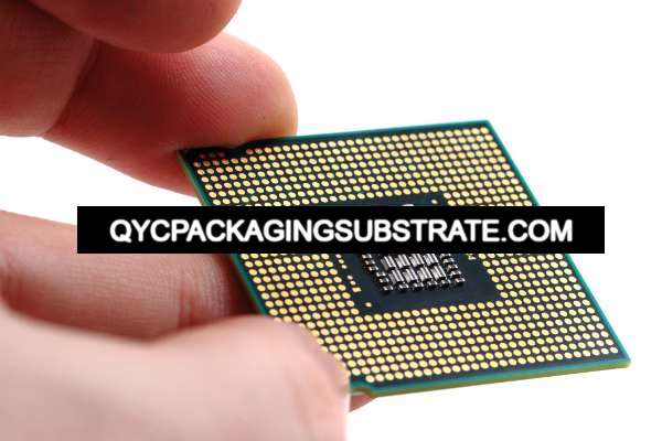
Radio Frequency Cavity PCB Manufacturer. High speed and high frequency material Cavity PCBs, or Cavity BGA packaging substrate Vendor. Advanced Cavity production process.
In the context of today’s continuous development of electronic technology, the role of RF cavity PCB manufacturers in the electronics industry has become increasingly important. RF cavity PCB plays a key role in the fields of communications, radar, satellites and wireless networks. Its excellent RF characteristics and stability have become the first choice for various high-frequency electronic equipment. This article will delve into the importance of RF cavity PCBs and their widespread use in electronic devices.
What is Radio Frequency Cavity PCB?
Radio Frequency Cavity PCB (Radio Frequency Cavity PCB) is a printed circuit board specially used to process radio frequency signals. Compared with traditional printed circuit boards, RF cavity PCBs have special design and manufacturing requirements to ensure excellent performance and stability at high frequencies.
This type of PCB usually uses special materials and structures to reduce signal loss and interference and provide good radio frequency characteristics. One of its notable features is that it has a cavity or hole structure inside. This design helps reduce the propagation path of electromagnetic waves, thereby reducing the loss of transmitted signals.
The design of RF cavity PCB needs to consider factors such as layout, layer stacking, conductor width, and impedance matching to ensure stability and performance in high-frequency environments. In addition, material selection is also crucial. Commonly used high-frequency materials include special dielectric materials and low-loss copper foil to provide the best signal transmission effect.
RF cavity PCB is widely used in fields such as communications, radar, satellites and wireless networks, where the transmission requirements for high-frequency signals are very strict. Its excellent radio frequency characteristics and stability make it the first choice for various high-frequency electronic equipment.
Overall, RF cavity PCB plays an important role in modern electronic technology, and its special design and manufacturing requirements make it an ideal choice for processing high-frequency signals, providing reliable solutions for various RF applications.
Radio Frequency Cavity PCB design Reference Guide.
RF cavity PCB design is a complex and critical task to ensure that it provides excellent performance and stability in high-frequency environments. The following is a brief RF cavity PCB design reference guide designed to help designers overcome common challenges and achieve optimal designs.
Radio Frequency Cavity PCB Manufacturer
PCB layout and routing
The transmission of RF signals is greatly affected by layout and wiring. To minimize signal loss and crosstalk, use short, straight, wide cabling paths with as few turns and sudden changes as possible. When laying out, try to place RF components as close to each other as possible to reduce the length of the signal transmission path.
Impedance matching
Radio frequency signals need to maintain stable impedance matching during transmission to ensure the integrity and stability of signal transmission. During the design process, appropriate impedance matching should be performed based on the design requirements and circuit characteristics, and appropriate transmission line width and spacing should be used.
Layer stack design
RF cavity PCBs often feature multi-layer designs to provide better signal isolation and impedance control. In the layer stack design, the positions of signal layers, ground layers, and power layers should be properly arranged to minimize signal crosstalk and electromagnetic interference.
Material selection
PCB material is critical to RF performance. Commonly used materials include high-frequency glass fiber and special PTFE-based dielectric materials with low loss and stable dielectric constant. When selecting a material, factors such as its dielectric constant, loss factor, thermal stability and mechanical strength should be considered.
Electromagnetic Compatibility (EMC) Design
RF cavity PCB design should consider electromagnetic compatibility to minimize interference and sensitivity to the surrounding environment. Through appropriate layout, ground wire design, and layer stacking, radiated and conducted interference can be effectively reduced to ensure stable operation of equipment in high-frequency environments.
Thermal management
In high-frequency applications, thermal management is one of the important considerations in RF cavity PCB design. Through proper heat dissipation design and thermal conduction path planning, heat can be effectively removed and the stable operating temperature of circuit components can be maintained.
RF cavity PCB design is a complex and precise task that requires designers to have deep professional knowledge and experience. By following the above design guidelines, designers can overcome common design challenges and achieve optimal performance and stability of RF cavity PCB designs.
What material is used in Radio Frequency Cavity PCB?
Material selection for RF cavity PCB is critical to its performance. During the design and manufacturing process, appropriate materials can ensure that the PCB has excellent electrical performance and stability in high-frequency environments. The following are commonly used RF cavity PCB materials:
High frequency fiberglass
High frequency fiberglass is a premium substrate material with excellent dielectric properties and stability. It can provide good dielectric constant and dielectric loss, helping to maintain stable signal transmission, while having good mechanical strength and high temperature resistance.
Copper foil
Copper foil is a commonly used conductive layer material in RF cavity PCB. High-quality copper foil can provide good electrical conductivity and ensure signal transmission efficiency on the PCB. In addition, copper foil also has good welding properties, which helps the assembly process go smoothly.
Special dielectric materials
RF cavity PCBs often require special dielectric materials to achieve precise control and regulation of signals. These special dielectric materials have precise dielectric constant and dielectric loss, which can ensure the stability and accuracy of signal transmission in PCB. At the same time, these materials also have good high temperature resistance and chemical stability, making them suitable for long-term stable operation in harsh working environments.
By rationally selecting and combining these materials, RF cavity PCB manufacturers can achieve precise control of the PCB to ensure its excellent performance and reliability in high-frequency environments. The selection of these materials not only affects the performance of the PCB, but is also directly related to the stable operation of electronic equipment in radio frequency applications. Therefore, material selection is one of the crucial considerations when designing and manufacturing RF cavity PCBs.
What size are Radio Frequency Cavity PCB?
RF cavity PCBs are sized to suit specific application needs and can therefore be customized in a wide range of sizes. From micro packages to large boards, RF cavity PCB can meet the requirements of different scenarios.
For micro-packaged RF cavity PCBs, the size may be very small, even up to a few millimeters in size. This miniature package is suitable for RF applications in small electronic devices such as smart wearables and medical devices. The miniature size design makes these devices more lightweight and portable, and can implement complex RF functions in a limited space.
On the other hand, for the RF cavity PCB of a large board, its size may be larger, even reaching an area of tens or even hundreds of square centimeters. This large size is often used in communications base stations, radar systems, satellite communications and other equipment that need to process large amounts of radio frequency signals. The large size design provides enough space to accommodate complex circuit layouts and multiple RF components while maintaining good signal transmission and interference immunity.
In addition, RF cavity PCBs can be customized to meet the shape requirements of specific applications. In addition to the common rectangular shape, it can also be customized into circular, oval, or even irregular shapes to adapt to various special installation scenarios or mechanical structure requirements.
In summary, the flexible customization of the size and shape of RF cavity PCB makes it ideal for a variety of RF applications. Whether it is a micro package or a large board, it can meet the radio frequency signal processing needs in different scenarios, providing strong support for the performance improvement and innovation of electronic equipment.
The Manufacturer Process of Radio Frequency Cavity PCB.
The manufacturing process of RF cavity PCB is a highly complex and precise process, which involves multiple key steps and requires strict control and highly specialized technology from design to final assembly. The following is the basic process of RF cavity PCB manufacturing:
Design phase
The first step in manufacturing an RF cavity PCB is the design. At this stage, engineers use professional PCB design software to create circuit diagrams and layout designs based on customer requirements and circuit specifications. In the design of RF cavity PCB, special attention needs to be paid to the stability of signal transmission and the accuracy of impedance matching.
Prototyping
Once the design is complete, a prototype of the RF cavity PCB is produced. Rapid prototyping techniques such as printing and stripping are often used to quickly verify the correctness and feasibility of the design. The prototyping phase also includes preliminary testing and tweaking of the circuit board to ensure it meets design requirements.
Chemical corrosion
In the next step of PCB manufacturing, the raw copper foil surface is chemically etched to form the wires and connections required in the circuit diagram. The process involves coating copper foil on a fiberglass substrate and chemically etching away the excess, leaving the desired circuit pattern.
Drilling
Drilling holes in circuit boards are used to mount components and connect wires between different layers. RF cavity PCBs often require very precise aperture and positioning to ensure signal transmission quality and stability. Therefore, the drilling process must be very precise and tightly controlled on the PCB.
Assemble
The final stage is to mount the components on the PCB and solder them to complete the RF cavity PCB assembly. This involves precisely positioning components on the PCB via Surface Mount Technology (SMT) or Plug-in Technology (PTH) and connecting them to the PCB using soldering techniques. After assembly, the PCB will undergo rigorous testing and quality control to ensure its performance and reliability meet expected levels.
In general, the manufacturing process of RF cavity PCB is a highly specialized and precise process that requires the comprehensive use of design, process and technology to ensure the quality and performance of the final product. Through strict manufacturing processes and quality control, RF cavity PCB manufacturers are able to provide high-performance, stable and reliable products to meet the needs of different industries for RF electronic equipment.
The Application area of Radio Frequency Cavity PCB.
RF cavity PCB has a wide range of applications in fields such as communications, radar, satellites and wireless networks. In modern communication technology, RF cavity PCB plays a key role. Its excellent RF characteristics and stability make it the first choice for various high-frequency electronic equipment.
First of all, RF cavity PCB plays a vital role in the communication field. In mobile phones, base stations and satellite communication systems, RF cavity PCBs are widely used in the manufacturing of RF front-end modules, power amplifiers, filters, antennas and other components. Its high-frequency characteristics ensure stable transmission of signals, thereby ensuring the reliability and performance of the communication network.
In addition, radar systems are also one of the important application areas of radio frequency cavity PCB. Radar systems need to process a large number of radio frequency signals and have extremely high requirements for signal accuracy and stability. RF cavity PCB can provide excellent signal transmission and anti-interference capabilities, so it is widely used in radar transmitters, receivers and signal processing modules.
Satellite communications is another major application area for RF cavity PCBs. Satellite systems need to process a large number of radio frequency signals from ground stations and other satellites, and require the stability and reliability of signal transmission. RF cavity PCB plays an important role in satellite communication modules, navigation systems and remote sensing equipment, providing reliable guarantee for the normal operation of satellite communication systems.
In addition, wireless network equipment is also one of the important application areas of radio frequency cavity PCB. In Wi-Fi routers, Bluetooth devices and mobile communication equipment, RF cavity PCB is widely used in functional modules such as modulation and demodulation of RF signals, power amplification and antenna connection. Its stable radio frequency characteristics can ensure high-speed data transmission and stable connection of wireless network devices.
In short, RF cavity PCB, with its excellent RF characteristics and stability, has broad application prospects in the fields of high-frequency electronic equipment such as communications, radar, satellites and wireless networks, and provides important support for the development of modern communication technology.
What are the advantages of Radio Frequency Cavity PCB?
Compared with traditional wiring methods, RF cavity PCB (Radio Frequency Cavity PCB) has significant advantages in modern electronic equipment manufacturing. Here is a more detailed introduction to the advantages of RF cavity PCB:
Small size
RF cavity PCB design uses advanced layout and wiring technology to achieve a highly integrated and compact design of the circuit board. Compared with traditional wiring methods, RF cavity PCB occupies less space and can meet the demand for miniaturized electronic equipment, making the equipment lighter and more portable.
Stable performance
RF cavity PCB uses high-quality materials and precise manufacturing processes to provide stable electrical performance and signal transmission quality. Its excellent impedance matching and signal isolation capabilities ensure reliability and stability at high frequencies and reduce the risk of signal interference and distortion.
Easy to mass produce
The manufacturing process of RF cavity PCB has been carefully optimized to achieve high-efficiency mass production. Through automated equipment and process control, production costs can be reduced and production efficiency improved, thereby meeting the market’s demand for large quantities of electronic equipment.
Flexible design
The design flexibility of RF cavity PCB is extremely high and can be customized according to the needs of different applications. From layer stacking, impedance control to the layout of RF components, everything can be adjusted and optimized according to specific requirements, making RF cavity PCB adaptable to various complex circuit designs and system integration.
In general, RF cavity PCB has significant advantages in size, performance, production efficiency and design flexibility, and therefore plays a key role in the manufacturing of modern electronic equipment. It can meet the needs for high performance, high reliability and high integration, and promotes technological progress and application innovation in the fields of wireless communications, radar, satellites and wireless networks.
FAQ
What is the difference between RF cavity PCB and ordinary PCB?
RF cavity PCBs are specifically designed to handle high-frequency signals and have more stringent electrical performance requirements. Compared with ordinary PCBs, RF cavity PCBs usually use special materials and wiring techniques to ensure good signal integrity and anti-interference capabilities in high-frequency environments.
What is the design process of RF cavity PCB?
The design process of RF cavity PCB includes requirements analysis, schematic design, layout and routing, impedance matching, layer stacking and other steps. During the design process, special attention needs to be paid to the transmission characteristics of RF signals to ensure that the circuit layout and inter-layer connections meet RF transmission requirements.
What are the considerations in material selection for RF cavity PCB?
When selecting materials for RF cavity PCB, factors such as dielectric properties, loss factor, thermal stability, and processing technology need to be considered. Commonly used materials include PTFE (polytetrafluoroethylene), FR-4 and RO4003, etc. Select the appropriate material according to specific application requirements.
What are the size limits for RF cavity PCBs?
The size limitation of RF cavity PCB mainly depends on its frequency characteristics and electromagnetic wave propagation characteristics. In high-frequency environments, size will have an impact on signal transmission, so the size of the PCB needs to be determined according to specific RF requirements.