 Professional Flip-Chip Packaging Substrate Supplier

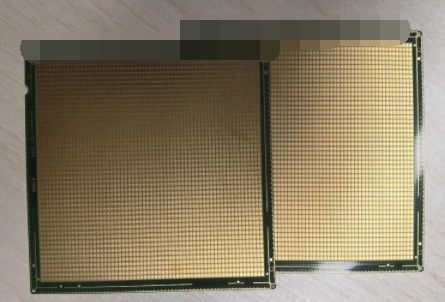
RF High Frequency Flip Chip Substrate Manufacturer. RF BGA package substrates Vendor, we produce the best samllest bump pitch with 100um, the best smallest trace and spacing are 9um. To use the High frequency and high speed materials, or other types BGA substrates materials.
As a core component of modern electronic equipment, PCB (Printed Circuit Board) plays a vital role in various industries. In the field of RF (radio frequency) high-frequency flip chip substrate manufacturing, PCB plays a key role. The manufacturing of RF high-frequency flip chip substrates requires precision design and advanced manufacturing processes to ensure stability and performance in high-frequency environments. In this article, we will delve into the key concepts of RF high-frequency flip chip substrate manufacturers and explain to you the importance of PCB and its application in the electronic field.
What is RF High Frequency Flip Chip Substrate?
RF high-frequency flip chip substrates are a vital component in today’s radio frequency (RF) electronic device manufacturing. It is a special printed circuit board (PCB) specifically designed for the manufacturing and integration of high-frequency radio frequency electronics. These devices include wireless communication equipment, radar systems, satellite communication equipment, and medical imaging equipment, etc., which need to handle the transmission and processing of high-frequency signals during their work. Compared with traditional PCB, the RF high-frequency flip chip substrate adopts a series of precise design and manufacturing processes to ensure stability and performance in high-frequency environments.
First of all, RF high-frequency flip chip substrates are usually made of materials with superior high-frequency characteristics, such as PTFE (polytetrafluoroethylene), FR-4 (glass fiber reinforced epoxy resin), etc. These materials have low dielectric loss, excellent dielectric constant stability and high high temperature resistance, which can effectively reduce losses during signal transmission and improve the signal-to-noise ratio and performance stability of the system.
Secondly, a series of precise manufacturing processes are used in the manufacturing process of RF high-frequency flip chip substrates. From design to manufacturing, every step requires precise calculation and strict control to ensure the dimensional accuracy of the board, the uniformity of the metal layer, and the accuracy of the connector. Especially in high-frequency environments, any slight asymmetry or mismatch may have a serious impact on signal transmission and processing, so the refinement and stability of the manufacturing process are crucial to product performance.
Finally, RF high-frequency flip chip substrates are widely used in high-frequency electronic equipment. Wireless communication equipment, including mobile phones, WiFi routers, base stations, etc., need to process the transmission and reception of high-frequency signals; radar systems need to process a large amount of high-frequency data in a very short time to achieve target detection and tracking; satellite communication equipment It requires the transmission and conversion of high-frequency signals between the earth and satellites; while medical imaging equipment needs to process high-frequency signals to achieve the collection and transmission of high-definition images. In these applications, the stability and performance advantages of RF high-frequency flip chip substrates have been fully demonstrated, providing a solid foundation for the development of modern high-frequency electronic equipment.
In summary, the RF high-frequency flip chip substrate, as a key component in the manufacturing of radio-frequency high-frequency electronic devices, provides important support for the development of high-frequency electronic equipment by using high-quality materials, precise manufacturing processes, and a wide range of application fields. and protection.
RF High Frequency Flip Chip Substrate
RF High Frequency Flip Chip Substrate design Reference Guide.
In the field of RF high-frequency flip chip substrate manufacturing, it is crucial to have a good reference guide. These guidelines not only guide manufacturers in making the right decisions during the design and production process, but also ensure that the final product’s performance and quality are as expected. Here are some key takeaways that are a vital reference guide for RF high frequency flip chip substrate manufacturers:
Be familiar with the characteristics of high frequency materials
RF high-frequency flipping chip substrates require the use of special high-frequency materials with good dielectric properties, low loss and stable performance. Manufacturers need to have a deep understanding of the properties of various high-frequency materials, including dielectric constant, dielectric loss, thermal stability, etc., in order to select the appropriate material for a specific application.
Master advanced design software and tools
In the design process of RF high-frequency flip chip substrates, it is crucial to use advanced design software and tools. These tools can help manufacturers perform high-frequency design, simulation analysis and layout planning to ensure that the design meets the performance requirements in high-frequency environments and has good signal integrity and EMI/EMC characteristics.
Learn about the latest manufacturing technologies and standards
With the continuous development of technology, the manufacturing technology of RF high-frequency flip chip substrates is also constantly updated. Manufacturers need to keep abreast of the latest manufacturing technologies and standards, including surface assembly technology, film processing technology, micro-fabrication technology, etc., to ensure that the production line is competitive and can meet customer needs and standard requirements.
For RF high frequency flip chip substrate manufacturers, the reference guide mentioned above is crucial. Only by in-depth study of the characteristics of high-frequency materials, mastering advanced design software and tools, and understanding the latest manufacturing technologies and standards, manufacturers can stand out in the highly competitive market and provide customers with high-performance, high-quality products.
Through continuous learning and accumulation of experience, manufacturers can continuously improve their manufacturing level and technical capabilities, and make greater contributions to the development and application of RF high-frequency flip chip substrates. It is hoped that this article can provide some useful reference and guidance for RF high-frequency flip chip substrate manufacturers and promote the development and progress of the industry.
What material is used in RF High Frequency Flip Chip Substrate ?
In the manufacturing process of RF high-frequency flip chip substrates, it is crucial to select appropriate materials, because the selection of materials directly affects the performance and reliability of the product. The following are some commonly used materials:
PTFE (polytetrafluoroethylene)
PTFE is a high-frequency material with excellent electrical properties and is widely used in the manufacture of RF high-frequency flip chip substrates. Its low dielectric constant and low loss tangent make signal transmission more stable and have lower dielectric loss, thus ensuring the transmission efficiency and accuracy of high-frequency signals.
FR-4
FR-4 is a glass fiber reinforced epoxy resin material. Although it is not as good as PTFE in the RF high-frequency field, it is still widely used in some low-frequency and medium-frequency applications. It has good mechanical strength and heat resistance and is suitable for some scenarios with less stringent performance requirements.
Metallized ceramics
Metallized ceramics are special materials with excellent high-frequency performance and dimensional stability. It is usually composed of a ceramic substrate and a metal layer. It can maintain stable electrical performance in extreme high-frequency environments and is therefore widely used in some applications that require extremely high signal transmission.
In addition to the above-mentioned common materials, there are also some special materials such as lithium zinc titanate (LTCC), polyimide (PI), etc., which can also play an important role in specific application scenarios. These materials usually have excellent high-frequency characteristics and dimensional stability, and are suitable for some fields with extremely high performance requirements.
To sum up, there are a wide variety of materials used in the manufacturing of RF high-frequency flip chip substrates, and each material has its specific advantages and applicable scenarios. Manufacturers need to select appropriate materials based on specific design requirements and application needs to ensure that products can provide stable and reliable performance in high-frequency environments.
What size are RF High Frequency Flip Chip Substrate?
When it comes to RF high frequency flip chip substrate size, flexibility and customization are key. This flexibility stems from its diverse application needs and the continuous development of industry standards. The size range of RF high-frequency flip chip substrates and their changes in different application scenarios will be discussed in more detail below.
Micro size chip level
For micro-size chip-level RF high-frequency flipping chip substrates, very precise design and manufacturing processes are usually required. This type of substrate may be used in small electronic products such as mobile devices, smart wearables, and sensors. In these applications, size and weight requirements are very stringent, so the substrate must be designed to be as small as possible to allow tight integration with other components and provide high-performance RF transmission.
Micro-sized chip-level substrates usually use advanced micro-slit and micro-line width manufacturing technologies to ensure good high-frequency performance and signal transmission characteristics. This type of substrate may have a complex multi-layer structure to achieve higher integration and better signal isolation.
Large size communication equipment level
Compared with micro-sized substrates, large-sized communication equipment-level RF high-frequency flip chip substrates are generally more complex and diverse. This type of substrate may be used in large equipment such as communication base stations, satellite communications, and radar systems. In these applications, the size of the substrate is usually larger to accommodate more functional modules and RF devices, and to provide more powerful signal processing and transmission capabilities.
Large-sized communication equipment-level substrates usually require more thermal management and mechanical strength issues to be considered to ensure stability and reliability in harsh environments. In addition, this type of substrate may need to support more complex signal transmission and processing needs, so the design and manufacturing processes may be more complex and sophisticated.
Application scenario requirements
In addition to micro and large sizes, the size of the RF high-frequency flip chip substrate may also be customized according to specific application scenarios and needs. For example, in military applications, substrates may need to have higher immunity to interference and greater mechanical strength; in medical devices, substrates may need to meet more stringent biosafety and reliability standards.
Therefore, the size design of the RF high-frequency flip chip substrate must fully take into account specific application requirements to ensure stable and reliable performance in a variety of environments and scenarios.
When manufacturing RF high-frequency flip chip substrates, it is crucial to understand its size requirements and application scenarios. Through flexible size design and precise manufacturing processes, manufacturers can provide customers with customized solutions that meet their specific needs, providing stable and reliable RF high-frequency flip chip substrates for various application scenarios.
The Manufacturer Process of RF High Frequency Flip Chip Substrate.
When it comes to the manufacturing process of RF high-frequency flip chip substrates, it involves multiple complex steps and links, each of which is crucial and directly affects the performance and quality of the final product. The manufacturing process of RF high-frequency flip chip substrate will be discussed in detail below.
Design
The first step in manufacturing an RF high-frequency flip chip substrate is design. During the design stage, factors such as the product’s functional requirements, circuit layout, and inter-layer connections need to be taken into consideration. With the help of advanced design software, engineers can accurately map out the wiring and component placement of each layer to ensure the performance and reliability of the final product.
Material selection
After the design is determined, the next step is material selection. RF high-frequency flipping chip substrate requires the use of materials with excellent high-frequency characteristics, such as PTFE (polytetrafluoroethylene). The choice of materials directly affects the high-frequency performance and signal transmission characteristics of the product, so it needs to be selected carefully.
Plate preparation
After selecting the material, proceed to plate preparation. This step includes cutting, milling, drilling and other processing processes on the board to ensure that the size and shape of the board meet the design requirements. Plate preparation requires high-precision equipment and technology to ensure the quality and stability of the plates.
Printing
Printing is one of the key steps in manufacturing RF high-frequency flip chip substrates. During the printing process, the copper foil layer is covered on the surface of the board, and the excess copper foil is removed using photolithography technology to form the required circuit and component structures. The precision and stability of the printing process directly affect the performance and reliability of the final product.
Assemble
The final step is assembly. During the assembly process, the components are accurately installed on the board according to the design requirements and fixedly connected through welding and other processes. The assembly process requires a high degree of precision and technical requirements to ensure accurate positioning of components and reliable connections.
Precise manufacturing processes and strict quality control are the keys to ensuring stable performance of RF high-frequency flip chip substrate products. Every manufacturing link needs to be strictly controlled to ensure product quality meets requirements. Only in this way can we produce high-quality RF high-frequency flip chip substrate products that meet customer needs.
Through the above steps, we can better understand the manufacturing process of RF high-frequency flipping chip substrates, as well as the key technologies and processes involved.
The Application area of RF High Frequency Flip Chip Substrate.
When it comes to the application field of RF high-frequency flip chip substrates, its importance and wide range of applications are impressive. These substrates play a vital role in fields such as wireless communications, radar, satellite communications, and medical equipment, and their stable performance and reliability provide a solid foundation for these fields.
Wireless communication
In the field of wireless communications, such as 5G and the Internet of Things (IoT), RF high-frequency flip chip substrates are widely used to manufacture high-frequency, high-speed, and low-latency communication equipment. These substrates can help achieve faster data transmission and more stable signal transmission, thus promoting the development of wireless communication technology.
Radar
In radar technology, RF high-frequency flip chip substrates are used to manufacture high-performance radar systems. These systems play a key role in the fields of military, aerospace, and meteorology, and can achieve functions such as long-range detection, precise target identification, and tracking.
Satellite Communications
Satellite communications are an important part of modern communications networks, and RF high-frequency flip chip substrates are the core of satellite communications systems. These substrates can maintain stable performance in harsh space environments and ensure reliable operation of satellite communication systems.
Medical equipment
In the field of medical equipment, RF high-frequency flip chip substrates are widely used in key equipment such as medical imaging equipment, wireless monitoring equipment, and life support systems. These substrates can ensure stable operation of equipment and accurate data transmission, playing a vital role in medical diagnosis and treatment.
In summary, RF high-frequency flip chip substrates are widely used in fields such as wireless communications, radar, satellite communications, and medical equipment. Its stable performance and reliability provide a solid foundation for these fields. With the continuous advancement of technology and the expansion of application fields, it is believed that RF high-frequency flip chip substrates will show their importance and value in more fields.
What are the advantages of RF High Frequency Flip Chip Substrate?
RF high-frequency flip chip substrate has significant advantages in modern high-frequency electronic equipment. Compared with traditional PCB, it shows more outstanding performance and characteristics in high-frequency environment, mainly reflected in the following aspects :
Better high frequency performance
The RF high-frequency flip chip substrate uses special high-frequency materials and adopts precise manufacturing processes to ensure stability and reliability in high-frequency environments. Its optimized design and layout can effectively reduce distortion and attenuation of signal transmission, thereby improving high-frequency performance and signal transmission rate.
Lower signal loss
Since the RF high-frequency flip chip substrate uses high-frequency materials and undergoes precise manufacturing processes, signal loss can be reduced during signal transmission. In contrast, traditional PCBs are prone to signal attenuation and loss in high-frequency environments, while RF high-frequency flip chip substrates can more effectively maintain signal stability and integrity.
Higher integration
RF high-frequency flipping of the chip substrate can achieve higher integration, that is, integrating more functions and components on the same substrate. This is due to its optimized design and layout that utilizes space resources more efficiently and enables a more compact arrangement of components, thereby increasing circuit integration and performance density.
Smaller size
RF high-frequency flip chip substrates usually have smaller sizes, which makes them particularly suitable for scenarios with high size requirements, such as mobile communication equipment, wireless sensor networks, etc. In contrast, traditional PCBs are not suitable for applications in space-limited environments due to their large size, while RF high-frequency flip chip substrates can better meet the size requirements of modern high-frequency electronic equipment.
To sum up, the RF high-frequency flip chip substrate has better high-frequency performance, lower signal loss, higher integration and smaller size, thereby better meeting the performance and requirements of modern high-frequency electronic equipment. size requirements. This makes it one of the first choices in wireless communications, radar, satellite communications, medical equipment and other fields, providing strong support and driving force for the development and innovation of the electronics industry.
FAQ
How to evaluate the performance parameters of RF high-frequency flip chip substrate?
The performance evaluation of RF high-frequency flip chip substrates mainly includes high-frequency characteristic testing, signal transmission testing, noise testing, etc. By using professional testing equipment and instruments, we can comprehensively evaluate the frequency response, signal loss, noise indicators, etc. of the substrate to ensure that the product’s performance meets the design requirements and customer needs.
Are the design and manufacturing of RF high-frequency flip chip substrates restricted by specific standards?
Yes, the design and manufacturing of RF high-frequency flip chip substrates usually need to follow a series of specific standards and specifications, such as IPC-6018, IPC-6012, etc. These standards cover requirements in PCB design, material selection, manufacturing process, quality control, etc. to ensure product reliability and stability. Our manufacturing team strictly follows these standards to ensure product quality and performance meet industry standards and customer requirements.
How to ensure quality and reliability in supply chain management of RF high-frequency flipping chip substrates?
Our supply chain management team has taken a series of measures to ensure the quality and reliability of our supply chain. This includes supplier evaluation and auditing, raw material inspection, process control and quality tracking. By establishing a sound supply chain management system, we are able to detect and solve potential problems in a timely manner, ensuring product quality and delivery reliability.
What is the difference between RF high-frequency flip chip substrate and traditional PCB?
There are obvious differences between the RF high-frequency flip chip substrate and traditional PCB in material selection, manufacturing process and performance characteristics. First of all, RF high-frequency flip chip substrates usually use high-frequency materials, such as PTFE (polytetrafluoroethylene), etc., to meet performance requirements in high-frequency environments; while traditional PCBs use more conventional materials such as FR-4. Secondly, the RF high-frequency flip chip substrate is more precise in design and manufacturing process to ensure stability and reliability in high-frequency environments. Finally, in terms of performance characteristics, the RF high-frequency flip chip substrate has better high-frequency characteristics, lower signal loss and higher integration, and is suitable for application scenarios that require high high-frequency performance.