 Professional Flip-Chip Packaging Substrate Supplier

Semiconductor Glass Package Substrates Manufacturer. We use advanced Msap and Sap technology to produce the Glass Package Substrates with microtrace and minimum clearance, We have experience in glass substrate production.
In modern electronic equipment, semiconductor glass packaging substrates are an indispensable component. As a core component that connects various electronic components and provides electrical connections, it performs critical functions. This article will provide an in-depth study of the design, manufacturing and application of semiconductor glass packaging substrates, aiming to provide readers with a comprehensive understanding and in-depth insights.
What is the definition of semiconductor glass packaging substrate?
Semiconductor glass packaging substrate is a key electronic component used to support and connect semiconductor chips, which plays a vital role in modern electronic devices. This substrate is usually made of glass material, and its main function is to provide stable mechanical support and electrical connections so that the semiconductor chip can work effectively and communicate with other components.
The main components of semiconductor glass packaging substrate include glass substrate, conductive layer, insulating layer and covering layer. The glass substrate is the base material, providing a solid platform to support and hold chips and other components. The conductive layer is usually composed of a thin metal film and is used to transmit electronic signals and energy. The insulating layer plays the role of isolation and protection to prevent short circuit or leakage between the conductive layers. Finally, an overlay is typically a protective coating used to protect the substrate from dust, moisture, and other external environmental factors.
Designing semiconductor glass packaging substrates requires consideration of multiple factors, including circuit layout, signal integrity, thermal management, and mechanical strength. Good design can ensure that the substrate has good electrical properties, stable operating temperature, and reliable mechanical connections, thereby improving the performance and reliability of the entire electronic device.
During the manufacturing process, semiconductor glass packaging substrates usually undergo multiple process steps, including glass substrate preparation, metallization, chemical etching, printing, covering and final testing. Each step requires highly sophisticated equipment and technology to ensure the quality and performance of the substrate meet requirements.
Overall, semiconductor glass packaging substrates play an integral role in modern electronic manufacturing. By understanding its definition, composition, design and manufacturing processes, we can better apply and optimize this key technology, thereby promoting the development and innovation of the electronics industry.
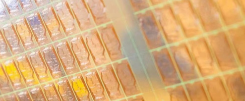
Semiconductor Glass Package Substrates
How is the semiconductor glass packaging substrate designed?
The design of semiconductor glass packaging substrates is a precision engineering task involving multiple critical steps and considerations. The following is a typical design process:
Requirements analysis and planning: First, the design team needs to communicate with customers or internal teams to understand the functional requirements and performance indicators of the product. This may include circuit functionality, dimensional requirements, operating environmental conditions, etc. Based on these requirements, the design team will formulate a design plan and determine basic parameters such as the number of layers, size, and materials of the substrate.
Schematic design: The design team draws schematic diagrams based on the circuit requirements of the product. In this step, they select the appropriate components and connect them into the circuit diagram. This requires consideration of the circuit’s function, layout, and wiring rules to ensure circuit performance and stability.
Place and route design: The next step is to convert the schematic into an actual place and route design. The design team will arrange the location of components on the substrate and draw wire routes to ensure the accuracy and stability of signal transmission. At this step, they need to consider factors such as signal integrity, electromagnetic compatibility (EMC) and thermal management.
Simulation and verification: Design teams use simulation tools to verify designs. They simulate the operation of the circuit to ensure it meets performance requirements and resolve possible problems. This may include signal interference, power consumption analysis, thermal analysis, etc. Once verified, the design team is ready to move to the next phase.
Design file generation: After the design is completed, the design team will generate the required design files, including schematics, layout and routing files, Gerber files, etc. These files will be used in subsequent manufacturing and production processes.
Design Review and Optimization: The design team conducts internal reviews and communicates with clients or other stakeholders to ensure the design meets all requirements. If needed, they make further optimizations and modifications to improve the performance and reliability of the design.
In general, the design of semiconductor glass packaging substrates is a comprehensive engineering task that requires the design team to have extensive experience and expertise. Through careful planning, design and verification, the design team can ensure that the final design meets product requirements and has excellent performance and stability.
What is the manufacturing process of semiconductor glass packaging substrates?
The manufacturing process of semiconductor glass packaging substrates is a precise and complex project, which requires precise coordination of multiple steps and highly technical implementation. The following is an overview of the manufacturing process of a typical semiconductor glass packaging substrate:
Before the manufacturing process can begin, design preparations first need to be carried out. This includes determining product specifications, selecting appropriate glazing materials and determining design layout. Design engineers use CAD software to create design files and ensure compliance with customer requirements and industry standards.
The first step in the manufacturing process is to prepare the substrate. The substrate is usually made of materials such as silicon, glass or ceramics. At this stage, the substrate is cleaned, cut and polished to ensure a smooth and flawless surface.
After the substrate is prepared, the next step is to clean the substrate and perform necessary surface treatment. This can include processes such as chemical treatments, laser drilling and metallization to ensure good adhesion and conductivity on the substrate surface.
Once the substrate is ready, the next step is to apply a glass layer on the substrate. This is usually achieved through techniques such as physical vapor deposition (PVD) or chemical vapor deposition (CVD). The quality and thickness of the glass layer are critical to the performance of the final product, so preparation parameters need to be tightly controlled.
After the glass covering is completed, the next step is to apply copper foil on the glass layer. Copper foil is a key material used for circuit connections. It can be applied to glass surfaces through methods such as electroless copper plating or vacuum deposition.
Once the copper foil is applied, the next step is to form the circuit. This involves using photolithography to transfer the circuit pattern on the design file to the surface of the substrate, and removing unwanted portions of the copper foil through chemical etching or lasers.
After the circuit is formed, the substrate enters the metallization and terminal processing stages. This involves depositing a metal layer onto the circuit surface to provide conductivity and, if necessary, applying a termination treatment to improve soldering performance.
Finally, the fabricated semiconductor glass packaging substrate will be submitted for final testing and quality control. This includes rigorous inspection of aspects such as circuit connectivity, insulation and dimensional accuracy to ensure the product meets specifications and meets expected performance requirements.
Through this manufacturing process, semiconductor glass packaging substrates achieve high quality and reliability, providing stable support and connections for a variety of electronic applications.
In what fields can semiconductor glass packaging substrates be used?
Semiconductor glass packaging substrates are widely used in various fields, and their flexibility and customizability make them an indispensable component in many electronic devices. The following are the applications of semiconductor glass packaging substrates in several major fields:
In communication equipment, semiconductor glass packaging substrates are widely used in manufacturing routers, switches, optical fiber communication equipment, etc. These devices require high-performance, high-density circuit boards to support data transmission and processing, and semiconductor glass packaging substrates are ideal for meeting these requirements. Its excellent high-frequency characteristics and good signal integrity make it the first choice for communication equipment manufacturers.
In computer hardware, semiconductor glass packaging substrates are used to manufacture key components such as motherboards, graphics cards, and memory modules. As computer performance continues to improve, the performance and stability requirements for circuit boards are also getting higher and higher. Semiconductor glass packaging substrates can provide excellent thermal management and signal transmission characteristics to ensure stable operation of computer systems.
In automotive electronic systems, semiconductor glass packaging substrates are widely used to manufacture automotive electronic control units (ECUs), in-vehicle entertainment systems, driving assistance systems, etc. The automotive industry has extremely high requirements for high temperature resistance, vibration resistance and reliability of electronic equipment, and the excellent performance of semiconductor glass packaging substrates can meet these requirements and help improve the performance and safety of automotive electronic systems.
In medical equipment, semiconductor glass packaging substrates are used to manufacture medical imaging equipment, life monitoring equipment, surgical auxiliary equipment, etc. These devices have extremely high requirements for the stability and precision of electronic components, and semiconductor glass packaging substrates can provide reliable electrical connections and precise signal transmission, thereby ensuring the accuracy and reliability of medical equipment.
In short, semiconductor glass packaging substrates are widely used in communications, computers, automobiles, medical and other fields, and with the continuous advancement of technology, their application scope in various fields will be further expanded.
How high is the cost of semiconductor glass packaging substrate?
The cost of semiconductor glass packaging substrates is a critical issue, especially for manufacturers and designers. So, let’s take a deeper look at this issue.
First of all, the cost of semiconductor glass packaging substrates is affected by many factors. One of the most important factors is the choice of materials. Different types of materials have different costs, and in some cases, require special handling and processing, which can increase costs. In addition, the size, thickness and number of layers of the substrate will also have an impact on cost. Generally speaking, larger size, thicker substrates and more layer designs will increase costs.
Secondly, the manufacturing process is also one of the important factors affecting cost. The manufacturing process of semiconductor glass packaging substrates involves multiple complex steps, including substrate preparation, glass covering, metallization and final testing. Each step requires specialized equipment and technology and may add cost. In addition, precision and quality control during the manufacturing process also have an impact on costs.
In addition, economies of scale are also one of the important factors affecting costs. Typically, large-scale production results in lower unit costs because fixed costs can be spread over more products. Therefore, for large-volume production orders, manufacturers usually offer more competitive prices.
Finally, market supply and demand will also have an impact on costs. Supply chain tensions and material price fluctuations can lead to cost fluctuations. In addition, market competition and industry development may also affect cost levels.
To sum up, the cost of semiconductor glass packaging substrates depends on many factors, including material selection, manufacturing process, scale efficiency and market supply and demand. In order to reduce costs and improve competitiveness, manufacturers and designers need to consider these factors and find the best solutions.
Who will manufacture the semiconductor glass packaging substrate?
In the process of manufacturing semiconductor glass packaging substrates, choosing the right manufacturer is crucial. As a technologically advanced and experienced company, we are committed to providing high-quality semiconductor glass packaging substrates and meeting the various needs of our customers.
As a manufacturer, we have advanced production equipment and a technical team that enable us to provide a full range of services from design to production. We use advanced manufacturing processes to ensure product quality and stability. Our production lines are highly automated and precisely controlled to meet orders of all sizes and ensure timely delivery.
In addition to technical strength, we also focus on customer needs and communication. Our team adheres to the concept of “customer first” and always puts the needs of our customers first. We provide personalized customization services and produce according to customer requirements to ensure the best results for each project.
In the manufacturing process of semiconductor glass packaging substrates, we not only focus on product quality, but also on environmental protection and sustainable development. We use environmentally friendly materials and processes, are committed to reducing our impact on the environment, and continuously optimize our production processes to improve resource utilization.
All in all, as a manufacturer, we have rich experience, advanced technology and a professional team, able to provide customers with high-quality semiconductor glass packaging substrates and achieve win-win cooperation. We look forward to working with you to jointly promote the development of the industry and achieve common value goals.
What are the five key attributes of great customer service?
In the semiconductor glass packaging substrate industry, providing excellent customer service is crucial. Here are five key qualities of great customer service:
Professionalism: Professionalism is the cornerstone of customer service. In the semiconductor glass packaging substrate industry, customers often require customized solutions for specific needs. Therefore, providing professional technical advice and support is crucial. A high-quality customer service team should have extensive industry knowledge and experience, be able to accurately understand customer needs, and provide corresponding technical advice and solutions.
Timely response: In a highly competitive market environment, timely response to customer needs is crucial. Customers may encounter various problems or have urgent needs during the project development process, so quick response can effectively improve customer satisfaction. A high-quality customer service team should establish effective communication channels and maintain timely communication and feedback to ensure that customers receive timely support and assistance.
Personalized Care: Every client is unique and their needs and concerns may vary. Therefore, personalized care is key to improving customer experience. A high-quality customer service team should have a deep understanding of customer needs and preferences and provide customized services and solutions. Help customers achieve their business goals by building close partnerships, thereby enhancing customer loyalty and trust.
Problem-solving skills: During project development and production, customers may encounter a variety of technical and operational issues. Therefore, customer service teams need to have good problem-solving skills. They should be able to quickly identify the source of the problem and provide an effective solution. In the process of solving problems, timely communication and cooperation are also crucial to ensure that the problem can be solved as soon as possible and avoid adverse effects on project progress and quality.
Continuous improvement: Continuous improvement in customer service quality is key to maintaining a competitive advantage. A high-quality customer service team should keep an open mind, accept customer feedback and suggestions, and constantly optimize service processes and improve service quality. Through continuous improvement, we continuously improve customer satisfaction and loyalty, thereby winning more market share and customer trust.
To sum up, professionalism, timely response, personalized care, problem solving and continuous improvement are the five key qualities that make up great customer service. In the semiconductor glass packaging substrate industry, adhering to these qualities will help build good customer relationships and achieve long-term business success.
FAQs
What is the life cycle of semiconductor glass packaging substrates?
The life of semiconductor glass packaging substrates often depends on several factors, including material quality, manufacturing processes and environmental conditions. Generally speaking, a well-designed and manufactured semiconductor glass packaging substrate can have a service life of several years or even more than ten years. However, with the continuous development of technology and changes in market demand, the life of packaging substrates may be shortened due to technological advancements. Therefore, continuous technology updates and optimization are key to ensuring the performance and reliability of packaging substrates.
What is the thermal management of semiconductor glass packaging substrates?
In high-performance and high-density electronic devices, thermal management is a critical consideration. Semiconductor glass packaging substrates often use thermally conductive materials and designs to effectively disperse and remove heat to ensure normal operating temperatures for chips and other components. In addition, the ventilation holes and heat dissipation structures in the design can also help improve the heat dissipation effect. By comprehensively considering factors such as material selection, design layout, and heat dissipation structure, the heat of the packaging substrate can be effectively managed and the performance and reliability of the device can be improved.
How to choose a suitable semiconductor glass packaging substrate material?
Selection of a suitable semiconductor glass packaging substrate material depends on the requirements and limitations of the specific application. Commonly used materials include fiberglass reinforced epoxy (FR-4), polyimide (PI), polytetrafluoroethylene (PTFE), etc. FR-4 is a common base material that has good insulation properties and mechanical strength and is suitable for general applications. PI and PTFE have higher temperature stability and chemical stability, and are suitable for applications under high temperature, high frequency and special environments. Choosing the right material should take into account factors such as electrical performance, mechanical properties, temperature stability and cost.
How long is the manufacturing cycle of semiconductor glass packaging substrates?
The manufacturing cycle time for semiconductor glass packaging substrates varies depending on the manufacturer and order volume. Typically, the entire manufacturing cycle from design to delivery can take anywhere from weeks to months. Manufacturing cycle time is affected by multiple factors, including design complexity, material supply, process flow, and production equipment. In order to ensure timely delivery and meet customer needs, manufacturers usually adopt optimized production planning and flexible production scheduling.
What are the maintenance requirements for semiconductor glass packaging substrates?
Semiconductor glass packaging substrates usually do not require special maintenance, but care should be taken to keep them clean and dry during use. Regular inspection and maintenance of environmental conditions around equipment to prevent the ingress of dust, moisture, and other contaminants can help extend the life and performance of packaging substrates. In addition, regular inspection of the working status and heat dissipation effect of the equipment, and timely discovery and handling of possible faults and problems are also important measures to maintain the normal operation of the equipment.