 Professional Flip-Chip Packaging Substrate Supplier

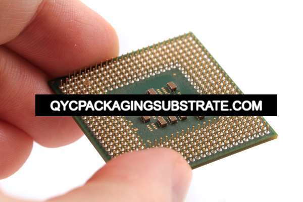
Semiconductor packaging substrate Firm. the Package Substrate will be made with Showa Denko and Ajinomoto High speed materials.
Semiconductor packaging substrates, a pivotal technological innovation in the electronics realm, assume a critical role by facilitating the connection of circuit components while offering protection and support. Going beyond a mere advanced electronic packaging substrate, they ingeniously merge rigid and flexible materials, delivering exceptional support and design flexibility for electronic product performance.
In our rapidly advancing technological era, the significance of semiconductor packaging substrates has become increasingly pronounced. What sets them apart is their ability to provide the stability akin to traditional rigid substrates while seamlessly incorporating the flexibility of pliable materials, thereby fostering diverse and innovative designs for electronic products. A primary advantage of this innovation lies in its ability to achieve high levels of circuit integration within confined spaces. This groundbreaking packaging method effectively addresses the limitations of traditional circuit boards in restricted spaces, providing a viable solution for the miniaturization and weight reduction of electronic devices.
The design flexibility inherent in semiconductor packaging substrates renders them widely applicable in various electronic products, be it smartphones, tablets, or medical devices. They ensure efficient electrical connections and stable support structures, enabling outstanding performance in a fiercely competitive market. The application scope of semiconductor packaging substrates extends beyond traditional consumer electronics, making inroads into emerging technology fields like the Internet of Things and artificial intelligence, thereby establishing a robust foundation for the evolution of future technologies.
The layer-by-layer stacking from Motherboard to Substrate includes circuit pattern preparation, chemical etching, blind hole drilling, metallization and other steps. Each step requires strict control and high precision. This ensures that the final product not only has excellent electrical properties, but also performs well in practical applications and is extremely reliable.
The advent and evolution of semiconductor packaging substrates have introduced fresh avenues for the design and production of electronic products. With its flexibility, highly integrated features, and extensive applicability across diverse fields, semiconductor packaging substrates emerge as the primary preference for electronic engineers. Looking ahead, as technology advances further, we anticipate that semiconductor packaging substrates will unveil their boundless potential across even more domains, infusing greater vitality and innovation into the future landscape of electronic technology.
What are the types of semiconductor packaging substrates?
The versatility of semiconductor packaging substrates positions it as a pivotal technology in the electronics industry, where different substrate types play crucial roles in meeting diverse design and application needs. Notably, rigid, flexible, and rigid-flexible substrates each exhibit distinct characteristics and advantages tailored to specific fields.
Semiconductor packaging substrate manufacturer
Rigid Substrate
Rigid substrates, typically fashioned from hard materials like fiberglass-reinforced epoxy (FR-4), are prevalent in PCB design. Widely employed in traditional electronic devices such as computer motherboards and graphics cards, their robust structure offers significant mechanical support. This sturdiness enables them to withstand substantial physical stresses, providing protection against damage induced by vibration.
Flexible Substrate
Flexible substrates, crafted from soft, thin materials like Mylar, offer a unique capacity to bend and fold. Suited for applications demanding high flexibility and bending properties, these substrates find utility in portable devices and curved screens. Their lightweight nature and adaptability allow for more flexible adaptations to designs of various shapes and sizes.
Rigid-Flexible Substrate
Rigid-flexible substrates ingeniously amalgamate the attributes of rigidity and flexibility into a comprehensive design. Rigid components provide support and secure electronic elements, while flexible sections facilitate interconnection and adaptation to special shapes. This substrate type excels in applications requiring high integration and spatial constraints, as seen in medical devices and aerospace systems.
Each semiconductor packaging substrate type boasts distinctive application areas and advantages. Rigid substrates, with their robust mechanical support, suit scenarios demanding stability and durability. The flexibility of flexible substrates proves valuable in compact, lightweight, and flexible designs. Rigid-flexible substrates provide an optimal solution without compromising performance, particularly in applications requiring high integration.
In conclusion, the diverse array of semiconductor packaging substrates offers a broad spectrum of choices for electronic product design. Engineers can dynamically select different substrate types based on specific application requirements, ensuring optimal performance and reliability.
What are the advantages of semiconductor packaging substrates?
Semiconductor packaging substrates, representing an advanced electronic packaging technology, bring forth distinct advantages when compared to traditional circuit boards, showcasing exceptional performance, flexibility, and reliability. Their notable strengths are prominently displayed in their ability to optimize space utilization, reduce weight, and enhance electrical performance.
A key highlight is the space efficiency offered by semiconductor packaging substrates. The reduced spatial footprint provided by semiconductor packaging substrates empowers designers with increased flexibility, facilitating superior optimization and innovation in both the aesthetics and functionality of products.
Furthermore, semiconductor packaging substrates demonstrate a significant advantage in weight reduction. Leveraging flexible materials and lightweight designs, these substrates inherently weigh less than their traditional counterparts, contributing to an overall reduction in product weight. This characteristic holds particular importance in applications with strict weight requirements, including drones, aerospace, and mobile devices, enhancing both product portability and performance.
Furthermore, semiconductor packaging substrates excel in electrical performance. Their design facilitates shorter signal transmission paths, minimizing signal attenuation and interference, thereby enhancing circuit stability and reliability. This is critically important for high-frequency and high-speed applications, such as communications equipment and high-performance computer systems. The excellent electrical properties of semiconductor packaging substrates ensure rapid and accurate signal transmission, enabling electronic products to perform effectively across diverse environments.
In summary, semiconductor packaging substrates bring forth a host of significant advantages to the field of PCB design through their distinctive design and material compositions. Amidst the trends of miniaturization, lightweight construction, and high performance, semiconductor packaging substrates have proven to be highly competitive and have evolved into an indispensable key technology in the realm of electronic product design.
Why choose semiconductor packaging substrates instead of other circuit boards?
Among various circuit boards, semiconductor packaging substrates distinguish themselves with unique design and performance benefits, offering substantial value and innovation in specific application domains. Let’s delve into a comprehensive exploration of why semiconductor packaging substrates are preferred over other options in certain applications.
Firstly, semiconductor packaging substrates excel in space utilization, thanks to their distinctive design. This enables higher-density circuit integration within confined spaces, making them particularly adept at achieving miniaturization and lightweight characteristics. For contemporary electronic products like smartphones and wearable devices, semiconductor packaging substrates meet design criteria for thinness, lightness, and compactness, enhancing portability to align with users’ practical needs.
Secondly, the flexible design of semiconductor packaging substrates presents optimal solutions for applications with specific shape and space constraints. In contrast to traditional rigid circuit boards, semiconductor packaging substrates exhibit greater flexibility, ensuring reliable circuit connections in intricate structures. This flexibility proves invaluable in meeting precise shape and space requirements, particularly in fields such as automotive electronics and medical devices.
Furthermore, the performance advantages of semiconductor packaging substrates constitute a key factor in their selection. They outperform other circuit boards in terms of signal transmission, electromagnetic compatibility, and heat dissipation. In high-frequency applications, semiconductor packaging substrates maintain signal stability more effectively, thereby enhancing overall system performance. Simultaneously, their superior heat dissipation capabilities effectively reduce temperatures in high-power applications, improving the reliability and lifespan of electronic equipment.
Additionally, the ongoing evolution of manufacturing processes and technologies for semiconductor packaging substrates provides more reliable solutions for mass production. Advanced manufacturing technologies and precise process control ensure consistent quality levels during mass production, mitigating manufacturing risks and reducing costs.
In summary, the unique design and performance advantages of semiconductor packaging substrates make them stand out in the realm of circuit boards. Specifically, in application areas such as mobile communications, medical electronics, and military equipment, semiconductor packaging substrates are chosen to pursue heightened performance, flexible design, and dependable electronic solutions.
What are the manufacturing processes for semiconductor packaging substrates?
In the semiconductor packaging substrate manufacturing process, design engineers play a crucial role by delving into the intricacies of both Motherboard and Substrate levels. Their profound understanding of these key steps is essential to ensure the ultimate product exhibits outstanding performance and reliability. The following provides a comprehensive overview of the primary stages in semiconductor packaging substrate manufacturing:
Design and Planning
At the outset, design engineers are tasked with formulating intricate design specifications and plans. This involves defining critical parameters such as the substrate’s physical dimensions, hierarchical structure, and circuit layout. Considerations extend to the functional requirements of the circuit, thermal management strategies, signal integrity, and other factors, all aimed at ensuring the final product is tailored to meet the demands of high-performance applications.
Material preparation
The use of high-quality materials is crucial during the Motherboard and Substrate manufacturing process. These materials include rigid and flexible substrates, conductive layers, dielectric layers, etc. Material selection directly affects the electrical performance, mechanical strength and durability of the substrate. Therefore, precise material preparation is the first step to ensure the quality of semiconductor packaging substrates.
Laminating and bonding
During the manufacturing process, rigid and flexible materials will be layered together to form an overall structure. This involves the layer-by-layer stacking of substrate layers, where the layers are firmly connected together with adhesives. Precision in this step is critical to ensuring the reliability and stability of the circuit.
Graphic layer preparation
In the production of motherboards and substrates, the creation of graphics layers entails the establishment of circuit patterns on the substrate’s surface. Typically achieved through a combination of photolithography and etching processes, this method ensures precise formation of the circuit pattern on the conductive layer of the substrate.
Chemical etching
After the circuit pattern is formed, chemical etching is required to remove excess metal. This step ensures a clear, precise circuit structure and avoids shorting between circuits due to excess conductor material.
Holes and metallization
Through blind hole drilling, manufacturing engineers form holes on the substrate that connect different levels to achieve interconnection of circuits. Afterwards, metallization is performed to enhance conductive properties and ensure smooth transmission of electrical signals within the substrate.
Final inspection and testing
The conclusive phase of the manufacturing process encompasses thorough inspection and testing of the semiconductor packaging substrate.
A more profound comprehension of these pivotal stages empowers design engineers to intricately grasp the semiconductor packaging substrate manufacturing process. This understanding, in turn, facilitates the optimization of designs, enhances production efficiency, and guarantees that the final product aligns seamlessly with the requirements of demanding applications. Such meticulous attention to these critical steps is instrumental in propelling innovation and fostering the development of cutting-edge electronic products.
What are the applications of semiconductor packaging substrates?
Semiconductor packaging substrates, a pivotal technology in the electronics sector, find widespread applications across various industries, providing robust support for the advancement and innovation of diverse equipment and systems.
The demands for heightened integration and miniaturization in modern smartphones make these substrates a fundamental component. Their rigid-flexible design enables accommodation of a multitude of electronic components within the confined internal space of mobile phones. From the main processor and graphics processing unit to various sensors, semiconductor packaging substrates facilitate substantial circuit integration through innovative design, allowing smartphones to maintain robust performance and functionality while retaining a slim and lightweight profile.
Similarly, in the domain of communication equipment, semiconductor packaging substrates assume a vital role. Whether for base station equipment or network routers, dealing with substantial data flows and intricate communication protocols is essential. These substrates enhance the efficiency of communication equipment through their high integration and reliability. Their combination of rigidity and flexibility enables adaptation to diverse layout requirements in varying environmental conditions. This adaptability ensures stable and efficient operation of communication equipment in diverse scenarios, facilitating seamless information transmission.
In the field of medical equipment, semiconductor packaging substrates play a key role due to the stringent requirements for stability, accuracy, and reliability. In medical imaging equipment, for instance, the high degree of integration and controllability of these substrates allows core components like image sensors and signal processors to collaborate, ensuring high-quality medical image output. Additionally, semiconductor packaging substrates are increasingly pivotal in emerging fields such as wearable medical devices and biosensors, providing innovative solutions for medical monitoring and treatment.
Collectively, the application cases of semiconductor packaging substrates in smartphones, communication equipment, and medical devices underscore their multifaceted and versatile characteristics. Their continual innovative designs and technological progress are poised to drive advancements across various industries, delivering greater convenience and innovation to our daily lives and work.
How to find a semiconductor packaging substrate manufacturer?
In the crucial quest for a reliable semiconductor packaging substrate manufacturer, the knowledge of effective approaches and recommendations becomes instrumental in ensuring success.
To initiate this search, it is advisable to explore semiconductor packaging substrate manufacturers through professional electronics industry exhibitions. These events serve as congregations for industry players, providing companies with valuable opportunities to showcase their products, technologies, and services. Engaging directly with various manufacturers at these exhibitions allows for a comprehensive understanding of their product lines, manufacturing capabilities, and cutting-edge production technologies. Furthermore, the exhibition serves as an ideal arena for establishing business relationships and networks, facilitating an initial screening process among multiple candidate manufacturers.
Secondly, use Internet resources, especially through online supply chain platforms or professional B2B websites, to find semiconductor packaging substrate manufacturers. These platforms provide detailed manufacturer information, product specifications and customer reviews, helping to objectively assess the credibility and strength of the manufacturer. Through online platforms, you can quickly access a large amount of information, reducing physical distance and time constraints, allowing potential manufacturers around the world to become candidates for partners.
Moreover, by actively engaging with industry associations and professional organizations, one can foster stronger connections through participation in industry seminars, conferences, and related activities. This not only offers valuable insights into the industry but also presents opportunities to identify potential semiconductor packaging substrate manufacturers. Associations often provide curated lists or recommendations of manufacturers, aiding in the focused selection of a partner that aligns more closely with specific needs.
In essence, employing a multi-faceted strategy that combines online and offline resources, along with a nuanced understanding of a manufacturer’s actual capabilities, is pivotal in pinpointing the semiconductor packaging substrate manufacturer that aligns best with the company’s requirements. Such a strategic selection not only addresses immediate needs but also establishes a resilient foundation for enduring and mutually beneficial collaboration in the future.
What is the quotation for semiconductor packaging substrates?
In today’s highly competitive electronics manufacturing landscape, the ability to secure precise and unequivocal quotes for semiconductor packaging substrates is paramount. This link not only directly impacts project costs and budgets but also exerts a profound influence on the overall production process and product quality. The following set of recommendations aims to assist readers in fostering effective communication with semiconductor packaging substrate manufacturers, ensuring the receipt of the most reasonable and transparent quotation information.
To begin, it is advisable to thoroughly assess the market reputation and historical performance of a semiconductor packaging substrate manufacturer before making a selection. Examining customer reviews, gauging industry reputation, and considering independent evaluations provide valuable insights into a manufacturer’s credibility and professionalism, forming a solid foundation for the decision-making process.
Clarity about your specific needs is crucial when communicating with manufacturers to secure an accurate quote. Clearly articulating design requirements, material preferences, production quantities, and lead times enables manufacturers to more precisely evaluate costs and tailor their quotes accordingly. Simultaneously, keeping manufacturers updated on any changes is essential for maintaining the accuracy of the quote.
Understanding the manufacturer’s pricing strategy is also pivotal. Familiarity with elements like volume discounts, offers for regular customers, and other pricing policies allows for a more nuanced evaluation of costs and establishes the groundwork for future relationships.
Providing comprehensive design documents and specifications to the manufacturer is another critical step. Precise design documentation aids manufacturers in gaining a thorough understanding of the project’s technical requirements, facilitating a more accurate assessment of production costs. This phase also allows the technical teams from both parties to engage in in-depth communication, resolving potential technical challenges and ensuring the precision of the quotation.
In an era rife with challenges and opportunities, obtaining accurate quotations for semiconductor packaging substrates stands as a key determinant of project success. Through these recommendations, readers are encouraged to engage with manufacturers more confidently and efficiently, fostering successful project implementation.
Frequently Asked Questions (FAQs)
Why choose Semiconductor Packaging Substrate in PCB design over other boards?
Semiconductor Packaging Substrate is chosen in PCB design for its unique design structure, making it suitable for applications with space constraints or complex shapes. It not only provides high customization but also enables more flexible designs in high-density circuit layouts.
How to obtain quotes for Semiconductor Packaging Substrate?
To obtain quotes for Semiconductor Packaging Substrate, it is recommended to directly communicate with multiple manufacturers. Provide clear design specifications and requirements to ensure accurate quoting information.
What factors should be considered when requesting a quote for Semiconductor Packaging Substrates?
Obtaining accurate quotes is crucial for project planning. We discuss factors to consider and provide guidance on ensuring transparent communication with manufacturers to obtain precise and comprehensive quotes.
Are there any design considerations or common challenges when working with Semiconductor Packaging Substrates?
We address common concerns related to design, emphasizing factors such as bending radius, transition zones between rigid and flexible sections, and interlayer connection methods. This information ensures a smoother integration of Semiconductor Packaging Substrates into the design process.
Where can one find Semiconductor Packaging Substrate manufacturers?
Understand effective methods and suggestions for locating reliable Semiconductor Packaging Substrate manufacturers, including considerations for choosing the right supplier for specific needs.
How is Semiconductor Packaging Substrate manufactured?
The manufacturing process involves crucial steps on both the motherboard and substrate levels. We provide insights into key manufacturing processes, ensuring a clear understanding of the production process.
Where can one find Semiconductor Packaging Substrate manufacturers?
Discovering reliable Semiconductor Packaging Substrate manufacturers is a vital step in the market. We share effective methods and advice to help readers find manufacturers that suit their specific needs.