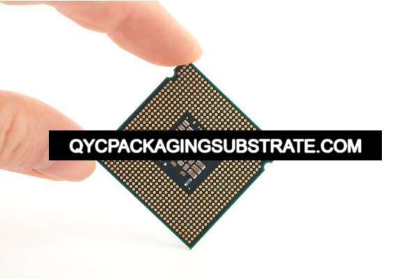
 Professional Flip-Chip Packaging Substrate Supplier

Advance Semiconductor substrate Vender. the Package Substrate will be made with BT, Showa Denko and Ajinomoto High speed materials.
Marked by an unwavering commitment to meeting the pressing demands for miniaturization, high performance, and heightened reliability in modern electronic devices, the Advanced Semiconductor Substrate introduces cutting-edge manufacturing processes and materials. It enhances the traditional role of a semiconductor substrate by incorporating innovative techniques to address the ever-evolving landscape of electronic engineering.
An essential attribute of the Advanced Semiconductor Substrate lies in its exceptional level of integration. By leveraging sophisticated manufacturing technologies, this substrate seamlessly incorporates a myriad of electronic components and connections. This heightened integration empowers more sophisticated functionalities within a confined space, enabling compact circuit designs and enhancing the overall performance of electronic devices.
Crucially, this semiconductor substrate maintains an impressive balance between high integration and excellent electrical performance. Its distinctive characteristics include low resistance, low inductance, and high thermal conductivity, contributing to the reduction of power consumption in circuits and the enhancement of signal transmission efficiency. These attributes play a pivotal role in meeting the stringent power consumption and performance requirements of modern electronic devices.
Advance Semiconductor Substrate provides PCB engineers with broader design flexibility. Due to its highly integrated nature, engineers can layout and design circuits more freely to achieve more complex functions. In addition, this substrate supports advanced packaging technologies, making equipment easier to repair and upgrade.
Advance Semiconductor Substrate plays a key role in various electronic devices. From smartphones to computers to communication devices, its high level of integration and superior performance drive innovation in modern electronic devices. This substrate is particularly suitable for applications with extremely high volume and performance requirements, such as portable devices and embedded systems.
Advanced Semiconductor Substrate stands as a pioneering technology in the realm of electronic engineering. Its remarkable attributes, including unparalleled levels of integration, superior electrical performance, and heightened design flexibility, empower PCB engineers with potent tools to forge cutting-edge and compact electronic devices in the dynamic market landscape. As manufacturing technology progresses, the pivotal role of Advanced Semiconductor Substrate in the electronics sector is poised to persist, propelling the industry into a future characterized by continuous innovation and advancement.
Rigid-fleAdvance Semiconductor substrate manufacturer manufacturer
What types of Advance Semiconductor Substrate are there?
In the dynamic landscape of today’s electronics industry, Advanced Semiconductor Substrates play a pivotal role, offering diverse types that afford extensive design possibilities for PCB (Printed Circuit Board) projects. This article aims to explore various Advanced Semiconductor Substrate types, including BGA (Ball Grid Array) and CSP (Chip Scale Package), delving into their distinctive features and analyzing their advantages in meeting diverse application scenarios and performance requirements.
BGA (Ball Grid Array)
BGA stands out as a prominent Advanced Semiconductor Substrate, renowned for its unique ball pad layout. This layout enhances density and facilitates superior heat dissipation for semiconductor devices. The incorporation of small balls beneath the substrate provides significant advantages in terms of integration and thermal conductivity.
The BGA design contributes to device compactness, reducing overall size and rendering it ideal for applications where space is a critical constraint. Furthermore, the spherical pad structure enhances welding reliability, mitigating issues arising from thermal expansion.
CSP (Chip Scale Package)
CSP emerges as another crucial Advanced Semiconductor Substrate, designed to encapsulate the chip in a package comparable to its size. Key attributes of CSP include its compact dimensions and lightweight design, making it the preferred choice for applications with stringent weight and space requirements.
CSP-type Advanced Semiconductor Substrates enhance device energy efficiency and reduce overall costs by minimizing package size and weight. This type finds applicability in portable devices, smart wearables, and scenarios demanding high standards of lightweight construction and miniaturization.
Advantages and Application Scenarios
Each type of Advanced Semiconductor Substrate brings unique advantages to distinct application scenarios. BGA excels in situations requiring high integration and heat dissipation performance, making it ideal for applications like high-performance computers and servers. On the other hand, CSP proves more suitable for lightweight, portable devices such as smartphones and wearables.
In summary, the choice between BGA and CSP depends on the specific requirements of the application, with considerations for integration, heat dissipation, size constraints, and weight playing pivotal roles in determining the most appropriate Advanced Semiconductor Substrate for a given project.
Both types meet the space efficiency, performance and reliability needs of different electronic devices through optimized designs. Manufacturers can select the appropriate Advance Semiconductor Substrate type based on specific application scenarios to achieve the best engineering design.
Among the many types of Advance Semiconductor Substrate, BGA and CSP are two important representatives that have attracted much attention. They are characterized by high integration, excellent heat dissipation performance, lightweight and miniaturized design, meeting the urgent needs of different electronic devices for performance and space efficiency. By in-depth understanding of the advantages and application scenarios of each type, PCB engineers can choose Advance Semiconductor Substrate in a more targeted manner to promote innovative development in the electronics field.
What are the advantages of Advance Semiconductor Substrate?
Advance Semiconductor Substrate is becoming a shining star in modern electronic design. Its superior advantages over traditional circuit boards provide unlimited possibilities for high-performance and compact design of various electronic devices. The following are three significant advantages of Advance Semiconductor Substrate, which build a solid foundation for it to be an ideal choice for modern electronic device design.
The advent of Advanced Semiconductor Substrate marks a pivotal breakthrough in electronic design, characterized by its compact and flexible nature. In stark contrast to traditional circuit boards, this innovative substrate allows for a substantially smaller footprint, enabling heightened device density and the incorporation of more functional components within confined spaces. Such advancements pave the way for the miniaturization and lightweighting of electronic products, delivering heightened portability and user comfort.
Beyond its smaller size, the Advanced Semiconductor Substrate boasts superior integration capabilities, facilitating the amalgamation of multiple functional modules on a diminutive substrate. This not only streamlines the electronic device design process but also mitigates system complexity. The resulting effect is a boost in production efficiency, empowering manufacturers with greater latitude to craft innovative and versatile smart devices laden with features.
Remarkably, the Advanced Semiconductor Substrate excels in thermal performance. Its cutting-edge materials and design enable efficient heat dissipation during high-load operations, preemptively averting overheating-induced damage to electronic components. This not only enhances the stability and reliability of electronic equipment but also lays the foundation for continuous improvements in device performance.
The appeal of the Advanced Semiconductor Substrate as an optimal choice for modern electronic equipment design lies not solely in its individual advantages but in the synergistic application of these features. The integration of numerous components onto a compact substrate empowers designers to intricately lay out components and paths, facilitating more precise circuit designs. This newfound flexibility fosters the creation of advanced, high-performance electronic devices, thereby propelling continuous innovation across the entire electronics industry.
In the dynamic landscape of electronic advancements, the Advanced Semiconductor Substrate stands as not just a technological leap but a catalyst for more intelligent, efficient, and reliable design solutions in electronic products. As technology perpetually evolves, this substrate is poised to maintain its leading role, steering the course of future electronic design with unwavering efficacy.
Why choose Advance Semiconductor Substrate over other boards?
In today’s rapidly developing electronics field, faced with a variety of circuit board options, Advance Semiconductor Substrate has attracted much attention as a leader. Why do companies and engineers prefer Advance Semiconductor Substrate to other circuit boards among many choices? Here’s a breakdown of the key factors.
The widespread acclaim for Advanced Semiconductor Substrate stems from its ability to meet the escalating demand for miniaturization and heightened integration in electronic devices. In the prevailing market trend favoring slimness, lightness, and portability, conventional circuit boards face limitations owing to their unwieldy size and layout constraints. Advanced Semiconductor Substrate adeptly addresses this challenge through its sophisticated manufacturing processes and reduced dimensions.
Simultaneously, its superior heat dissipation capabilities ensure stable equipment operation even under heavy workloads, providing robust support for a myriad of advanced electronic applications.
Within the realm of electronics, the extensively integrated Advanced Semiconductor Substrate serves as a catalyst for innovation and design. Relative to traditional circuit boards, its reduced size and stellar performance afford engineers increased design flexibility while addressing the imperative for electronic equipment miniaturization and heightened integration. This popularity extends across diverse application scenarios, with notable prevalence in smartphones, computers, communication equipment, and other sectors.
In essence, the preference for Advanced Semiconductor Substrate over alternative circuit boards stems not only from its advantages in miniaturization and heightened integration but also from its stellar electrical performance and reliability. These attributes collectively position Advanced Semiconductor Substrate as the premier choice for numerous electronic devices, ushering in fresh possibilities and opportunities within the field of electronic engineering.
What is the manufacturing process of Advance Semiconductor Substrate?
The production of Advanced Semiconductor Substrates involves a highly intricate and sophisticated process, leveraging a range of cutting-edge manufacturing technologies from design through production to ensure the resulting product attains high levels of quality and reliability. The foundational steps and pivotal technologies in Advanced Semiconductor Substrate manufacturing are outlined as follows.
Commencing with the design phase, engineers employ advanced CAD (Computer-Aided Design) software to meticulously craft the motherboard and backplane structure. This intricate design process necessitates profound technical expertise, addressing crucial aspects such as circuit layout, connection methods, and overall performance requirements.
The subsequent phase involves the meticulous preparation of raw materials. Specifically, advanced semiconductor materials, predominantly silicon-based, are meticulously chosen to guarantee the elevated stability and performance of electronic components. The quality and purity of these materials are paramount for ensuring the production of high-caliber Advanced Semiconductor Substrates.
At the core of the manufacturing process lies the production of circuits through lithography technology. Photolithography, a prevalent technique at this stage, involves coating the motherboard and bottom plate with a layer of photosensitive material. Subsequently, a photolithography machine exposes the pattern on the photosensitive material via mask projection. Techniques such as chemical etching or deposition then transfer the circuit pattern to the motherboard and backplane. The precision and stability of this step play a pivotal role in determining the performance of Advanced Semiconductor Substrates.
Upon reaching the packaging stage, the Advanced Semiconductor Substrate undergoes a meticulous process to safeguard specific circuit segments within a protective casing. This enclosure serves to shield the components from external elements, thereby augmenting the overall reliability of the circuit.
The final phase of the manufacturing journey involves rigorous quality control and testing procedures. Advanced semiconductor manufacturing facilities employ highly automated inspection apparatus to meticulously validate adherence to design specifications at each production stage. These thorough tests are instrumental in ensuring the uniformity of the manufacturing process and upholding the elevated quality and reliability standards of the eventual Advanced Semiconductor Substrate product.
In summary, the manufacturing process of Advanced Semiconductor Substrates seamlessly integrates cutting-edge CAD design, sophisticated lithography technology, precise metallization processes, and highly automated inspection procedures. This harmonious blend of advanced manufacturing technologies guarantees the consistent delivery of high-quality and reliable Advanced Semiconductor Substrates, offering unwavering and potent support for electronic devices.
Following circuit formation is the metallization step, wherein conductive paths and connections are established by depositing a metal layer onto the circuit’s surface. This stage commonly employs advanced metal evaporation or chemical vapor deposition technologies to ensure uniformity and conductivity of the metal layer.
In what application areas is Advance Semiconductor Substrate widely used?
In the realm of smartphones, the incorporation of Advanced Semiconductor Substrate heralds a new era of flexibility in mobile phone design. Capitalizing on its compact dimensions and heightened integration capabilities, it streamlines the layout of mobile phone chips, enabling the realization of an array of functions within constrained spatial confines. This extends beyond the optimized arrangement of processors and memory, encompassing the seamless integration of additional sensors and connectivity components in a more confined space. This not only augments the overall performance of the phone but also preserves a sleek and lightweight aesthetic.
Computer systems have increasing demands for high performance and high integration, and the superior performance of Advance Semiconductor Substrate makes it the first choice for solutions. By using this advanced substrate, computer motherboards can be designed more compactly while providing higher computing power and faster data transfer speeds. This means a faster, more efficient work experience for modern computer users.
The integration of Advanced Semiconductor Substrate in communication equipment has revolutionized the industry, rendering devices lighter and more portable. This innovation is pivotal in advancing mobile communications, network equipment, and various other communication technologies. The miniaturized design of Advanced Semiconductor Substrate not only alleviates the weight burden on communication equipment but also enhances overall performance and ensures a more reliable connectivity experience.
Its extensive application in these domains not only underscores the efficacy of Advanced Semiconductor Substrate in performance improvement but also serves as a cornerstone for the miniaturization design and innovative capabilities of electronic devices. Looking ahead, as this technology continues to evolve, we can anticipate Advanced Semiconductor Substrate taking a leading role in diverse fields, ushering in a wave of surprises and breakthroughs in electronic engineering.
Where to find Advance Semiconductor Substrate?
When pursuing Advance Semiconductor Substrate, choosing trustworthy manufacturers and suppliers is a key part of ensuring project success. Here are some suggestions to help you find a professional Advance Semiconductor Substrate manufacturer and how to obtain high-quality products and custom solutions.
Evaluating the credibility and experience of an Advanced Semiconductor Substrate provider is of utmost importance in the electronics industry. Opting for a well-established and reputable manufacturer increases the likelihood of understanding customer needs and delivering professional solutions. Experience is a key factor in comprehending and addressing the dynamic requirements of clients.
For projects that demand customized solutions, selecting a manufacturer with expertise in tailoring Advanced Semiconductor Substrate to specific requirements is imperative. Some manufacturers stand out in providing personalized solutions, encompassing aspects such as design, material selection, and process optimization.
Transparency in the supply chain is another critical factor. A trustworthy manufacturer should furnish transparent information regarding raw material sources, production processes, and quality control measures. This transparency ensures traceability and compliance with manufacturing processes for Advance Semiconductor Substrate.
Considering the historical collaboration between the supplier and the company is also pivotal. Assess the supplier’s track record in delivering high-quality Advance Semiconductor Substrate within stipulated timelines in past projects. A history of successful cooperation builds trust and facilitates the smooth execution of projects.
Examining reviews and feedback from other customers is a practical method to gauge a manufacturer’s performance. Real-life experiences of customers provide valuable insights into the manufacturer’s service levels and the quality of the Advance Semiconductor Substrate.
In summary, selecting a reliable Advance Semiconductor Substrate manufacturer is a crucial step in project success. Thoroughly evaluating the manufacturer’s reputation, product quality, customization capabilities, and historical collaboration with the supplier enables the identification of a partner that aligns with project needs, establishing a robust foundation for success.
What is the quote for Advance Semiconductor Substrate?
Since Advance Semiconductor Substrate is a highly advanced technology product, its price is usually relatively expensive. Knowing the typical price range for similar products on the market can help ensure your budget is reasonable and feasible.
In addition to general pricing, related factors are also affecting the specific quotation of Advance Semiconductor Substrate. Among them, material cost is a key factor. Advanced manufacturing materials and technologies often result in higher costs, but may also result in greater performance and reliability. Cost versus performance needs to be carefully weighed in purchasing decisions.
Given that these substrates often necessitate tailored production to meet the specifications of specific projects, customization may extend to design, processes, and specifications. It is imperative to clearly articulate your customization needs when engaging with the manufacturer and have a comprehensive understanding of the additional costs associated with these customization requirements. This clarity ensures a transparent and accurate quoting process.
Determining the proportion of Advance Semiconductor Substrate in the entire product cost helps to reasonably allocate the budget and ensure the economics of the overall project.
Finally, comparing different manufacturers and suppliers is also a critical step in getting the best quote. Different companies may use different production technologies, materials and supply chain strategies, which may result in different quotations. Through careful comparison, the most cost-effective solution can be found.
During the procurement process of Advance Semiconductor Substrate, an in-depth understanding of market pricing and related factors will help ensure that the budget is reasonable and ultimately make procurement decisions that meet project needs and economic benefits. This smart procurement method helps promote technological innovation and development in the field of electronic engineering.
Advance Semiconductor Substrate Frequently Asked Questions Need Answers?
What factors influence the pricing of Advance Semiconductor Substrate, and how can one make informed procurement decisions?
Understanding the general market pricing and relevant factors is essential when seeking quotes for Advance Semiconductor Substrate. This knowledge aids in budgeting and making informed decisions during the procurement process.
Are there any compatibility issues or considerations when integrating Advance Semiconductor Substrate into existing electronic systems?
Ensuring compatibility is crucial when integrating Advance Semiconductor Substrate into existing electronic systems. Considerations may include interface compatibility, power requirements, and communication protocols.
In which application domains does Advance Semiconductor Substrate find widespread use?
Advance Semiconductor Substrate finds extensive applications across a range of electronic devices, including smartphones, computers, and communication equipment. Understanding its role in enhancing performance and enabling size reduction is crucial for grasping its significance in various industries.
Where can one find reliable sources for Advance Semiconductor Substrate?
Reliable manufacturers and suppliers play a crucial role in sourcing Advance Semiconductor Substrate. The market hosts several specialized manufacturers offering high-quality products and customized solutions. Choosing reputable sources ensures the reliability and performance of the substrate in electronic designs.
How are the quotes for Advance Semiconductor Substrate determined, and what factors influence pricing?
Obtaining quotes for Advance Semiconductor Substrate involves understanding general market pricing and relevant influencing factors. This knowledge aids in budgeting and making informed procurement decisions. Factors such as customization requirements and market demand can impact the overall pricing structure.
How does the production timeline of Advance Semiconductor Substrate vary based on customization and manufacturing processes?
The production timeline of Advance Semiconductor Substrate depends on specific customization needs and the intricacies of manufacturing processes. Advanced production lines generally offer faster turnaround times, but customization and intricate requirements can influence the overall timeline.
In delving into these frequently asked questions, engineers and enthusiasts alike can gain a more comprehensive understanding of Advance Semiconductor Substrate’s nuances, fostering informed decision-making and driving innovation in the field of electronic engineering.