 Professional Flip-Chip Packaging Substrate Supplier

Substrate For Chips Manufacturer.”Substrate for chips manufacturer” refers to a specialized entity or facility dedicated to producing substrates used in chip manufacturing processes. These substrates serve as the foundational base upon which semiconductor chips are built. These manufacturers meticulously design and fabricate substrates with precise specifications to ensure optimal performance and reliability of the integrated circuits.
Chip substrate is a core component of modern electronic equipment and plays a vital role in the semiconductor industry. As a carrier of electronic components, the chip substrate realizes circuit functions by connecting various components to provide support for the normal operation of the device. Understanding the definition, design and manufacturing process of chip substrates, as well as its wide range of applications in various fields, is of great significance to practitioners in the electronics industry.
What is Substrate For Chips?
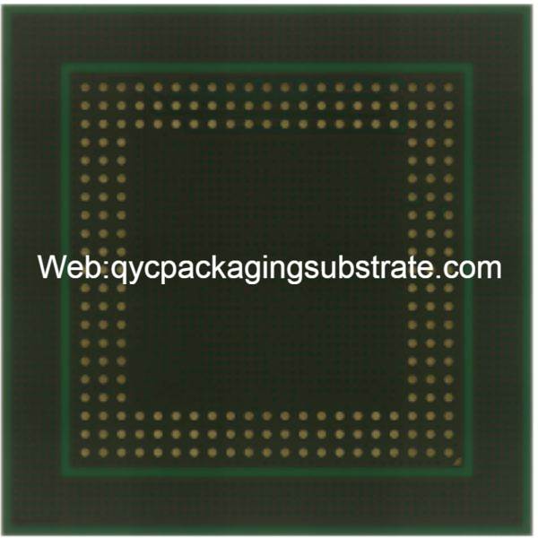
Chip substrate, also known as PCB (Printed Circuit Board), is a key electronic component that provides indispensable support for the operation of the modern technological world. It is a flat plate made of insulating material with various electronic components mounted on its surface and connected to each other through precise conductive paths to realize the function of the circuit. These conductive paths, pads and other features are etched from the copper foil covering the substrate, making the chip substrate one of the core components in electronic devices.
On the chip substrate, electronic components are precisely arranged and connected to build various circuits, from simple electronic products such as mobile phones and computers to complex industrial equipment and communication systems. Whether as personal consumer products or commercial applications, chip substrates play a vital role.
One of its key roles is to provide stable support and connections to ensure that electronic components can accurately transmit signals and data. In addition, the chip substrate can also achieve physical protection of the circuit and prevent damage to electronic components from the external environment.
Substrate For Chips Manufacturer
In addition, the design and manufacturing process of chip substrates is very complex and involves multiple processes and technologies. From material selection to circuit layout design to final production processing, highly specialized knowledge and skills are required. With the continuous advancement of technology, the manufacturing process of chip substrates is also constantly evolving to meet the needs of increasingly complex electronic products.
In general, chip substrates, as one of the cornerstones of modern electronic technology, bear huge responsibilities and missions. It not only connects various electronic components, but also connects the technological world that is ubiquitous in our daily lives.
Substrate For Chips design Reference Guide.
The Chip Substrate Design Reference Guide is a comprehensive handbook tailored for engineers and designers to provide best practices, design rules, software tools and techniques for chip substrate design to ensure design effectiveness and reliability.
In this guide, engineers and designers will find a collection of practical advice and guidance for chip substrate design. First, it provides design best practices for different types of chip substrates. Whether it is a rigid or flexible substrate, there are specific design requirements and constraints, and this guide will detail how to optimize the design to meet specific needs.
Second, this guide covers the design rules that are critical to ensuring proper functionality of the chip substrate. By following design rules, engineers and designers can avoid common design mistakes and ensure the reliability and stability of their designs.
In addition, this guide introduces a variety of software tools and techniques to assist in various stages of chip substrate design. From circuit design and layout to printing and assembly, engineers can streamline the design process and increase productivity by using advanced software tools and technologies.
Most importantly, this guide highlights key considerations and common challenges during the design process. By understanding these considerations, engineers and designers can better address various design challenges and ensure the quality and performance of their designs.
Overall, the Chip Substrate Design Reference Guide provides engineers and designers with a comprehensive handbook covering all aspects from design principles to practical applications. Both beginners and experienced professionals will gain valuable knowledge and insights to drive development and innovation in chip substrate design.
What material is used in Substrate For Chips?
Chip substrates are indispensable and critical components in electronic devices, and their material selection is critical to the performance and reliability of circuits. Typically, the main material used for chip substrates is FR4 (fiberglass reinforced epoxy laminate). FR4 is a substrate material composed of glass fiber and epoxy resin. It has excellent electrical insulation properties and mechanical strength and is suitable for the manufacture of a variety of electronic equipment.
The advantage of FR4 material is its stability and reliability, making it one of the preferred materials widely used in PCB manufacturing. In high-frequency and high-speed circuits, FR4 materials can provide good signal transmission performance and can withstand high temperatures and environmental pressures.
In addition to FR4, polyimide is also a commonly used chip substrate material, especially suitable for the manufacture of flexible chip substrates. Polyimide substrates have good flexibility and high temperature resistance, and are suitable for applications that require bending and deformation, such as flexible electronic products and curved displays.
In general, chip substrate material selection needs to be determined based on specific application needs and performance requirements. As two common substrate materials, FR4 and polyimide play an important role in the fields of rigid and flexible chip substrates respectively, providing reliable basic support for the manufacturing of various electronic devices.
What size are Substrate For Chips?
What is the size of the chip substrate? This is an application-specific issue. The size of the chip substrate depends largely on the scenarios it is used in and the requirements of the equipment. This is common from microchip substrates used in smartphones and wearable devices to large chip substrates used in industrial equipment or power electronics.
In smartphones and wearable devices, the chip substrate is usually very miniaturized due to the miniaturization requirements of the device itself. These devices need to free up as much space as possible to accommodate components such as batteries, screens, cameras, etc., so the size of the chip substrate is often relatively small. Microchip substrates may only be a few square centimeters in size, but they must be able to accommodate processors, memory, communication modules, and various sensors.
In contrast, industrial equipment or power electronics often require larger chip substrates. These devices may need to handle more complex circuits, including large power modules, heat sinks and other components, so the size of the chip substrate will increase accordingly. In these cases, the chip substrate may be tens or even hundreds of square centimeters in size to accommodate the large number of electronic components and ensure their proper operation and heat dissipation.
In general, the size of the chip substrate depends on the size of the electronic components and the space available within the device. Designers must try to control the size of the chip substrate within an appropriate range while meeting the functional requirements of the device to ensure the performance and reliability of the device.
The Manufacturer Process of Substrate For Chips.
The manufacturing process of chip substrates is a complex and precise process involving multiple key steps, each of which has an important impact on the quality and performance of the final product. The manufacturing process of the chip substrate will be introduced in detail below:
The first step in manufacturing a chip substrate is to prepare the substrate material. The commonly used substrate material is FR4, which is a fiberglass-reinforced epoxy resin laminate with good insulation properties and mechanical strength. In this step, the substrate material is cut to the required size and cleaned to remove surface dirt to ensure the smooth progress of subsequent process steps.
A thin layer of copper foil is deposited on the surface of the substrate to form a conductive layer in subsequent process steps. The copper layer can be deposited on the substrate surface by chemical or physical methods.
A layer of photoresist is coated on the surface of the copper foil and irradiated by an exposure light source, and the photoresist is partially cured using the pattern on the photoresist plate. This step will form a pattern on the photoresist that corresponds to the designed circuit board.
Through the etching process, the uncured photoresist and exposed copper foil are removed from the substrate surface, leaving the designed conductive paths and pads. This step usually uses a chemical etching method, in which the etching liquid gradually dissolves parts of the copper foil to form the desired conductive pattern.
Drills are drilled into the substrate using mechanical or laser drilling techniques at appropriate locations in order to mount electronic components and connect wires between different layers. These holes will be used for either PTH or blind via connections.
Precisely mount various electronic components such as chips, resistors, capacitors, etc. on the surface of the substrate. These elements will be placed in specific locations according to design requirements and installed using sophisticated automated equipment.
Electronic components are fixed on the substrate through surface mount technology (SMT) or plug-in technology and connected with wires. This usually involves a soldering process, where the component is firmly connected to the substrate by heating the solder so that it melts.
The manufactured chip substrate will undergo rigorous testing procedures to ensure that it meets the design requirements and has good performance and reliability. These tests may include electrical testing, functional testing, reliability testing, etc. to verify that all aspects of the chip substrate are working properly.
Through the above manufacturing process, the chip substrate is completed, providing a solid and reliable foundation for the normal operation of various electronic devices.
The Application area of Substrate For Chips.
Chip substrate, as a core component of modern electronic equipment, is widely used in various industries and plays a key role. Their application areas cover many fields such as consumer electronics, communications, automobiles, aerospace, medical equipment and industrial automation.
In the field of consumer electronics, such as smartphones, tablets, TVs, and game consoles, chip substrates play an important role in connecting and supporting various functions. Whether it is a processor, memory, communication module or sensor, a chip substrate is required as their basic support.
In the field of communications, including mobile phones, base stations, communication network equipment, etc., chip substrates are used to implement data transmission, signal processing and wireless communication functions. They must be designed and manufactured to meet stringent performance requirements to ensure the stability and reliability of communication networks.
The automotive industry is another important application area. Modern automobiles cover a large number of electronic systems, including engine control, in-car entertainment, safety systems and driver assistance technologies, etc., and these systems all require chip substrates to realize the connection and control of electronic components.
In the aerospace field, chip substrates are widely used in aerospace devices such as flight control systems, navigation equipment, communication systems, and satellites. Their high reliability and anti-interference ability are important considerations in the design of aerospace devices.
Medical devices are another important application area. From pacemakers and medical monitoring devices to medical imaging systems, chip substrates play a key role. They must be designed to meet the strict standards of the medical industry to ensure device safety and reliability.
Finally, in the field of industrial automation, chip substrates are widely used in equipment such as control systems, sensor networks, robots, and automated production lines. Their high performance and stability provide critical support for industrial production.
In general, chip substrates, as the basic building blocks of electronic devices, are ubiquitous and play a key role in various industries. Their applications range from consumer electronics to aerospace, from medical equipment to industrial automation, and are all-encompassing, making important contributions to the development and progress of modern science and technology.
What are the advantages of Substrate For Chips?
Chip substrate, as a core component of modern electronic equipment, is widely used in various industries and plays a key role. Their application areas cover many fields such as consumer electronics, communications, automobiles, aerospace, medical equipment and industrial automation.
In the field of consumer electronics, such as smartphones, tablets, TVs, and game consoles, chip substrates play an important role in connecting and supporting various functions. Whether it is a processor, memory, communication module or sensor, a chip substrate is required as their basic support.
In the field of communications, including mobile phones, base stations, communication network equipment, etc., chip substrates are used to implement data transmission, signal processing and wireless communication functions. They must be designed and manufactured to meet stringent performance requirements to ensure the stability and reliability of communications networks.
The automotive industry is another important application area. Modern automobiles cover a large number of electronic systems, including engine control, in-car entertainment, safety systems and driver assistance technologies, etc., and these systems all require chip substrates to realize the connection and control of electronic components.
In the aerospace field, chip substrates are widely used in aerospace devices such as flight control systems, navigation equipment, communication systems, and satellites. Their high reliability and anti-interference ability are important considerations in the design of aerospace devices.
Medical devices are another important application area. From pacemakers and medical monitoring devices to medical imaging systems, chip substrates play a key role. They must be designed to meet the strict standards of the medical industry to ensure device safety and reliability.
Finally, in the field of industrial automation, chip substrates are widely used in equipment such as control systems, sensor networks, robots, and automated production lines. Their high performance and stability provide critical support for industrial production.
In general, chip substrates, as the basic building blocks of electronic devices, are ubiquitous and play a key role in various industries. Their applications range from consumer electronics to aerospace, from medical equipment to industrial automation, and are all-encompassing, making important contributions to the development and progress of modern science and technology.
FAQ
What is the size of the chip substrate?
The size of the chip substrate varies depending on the application. They can be as small as used in microdevices, such as smartphones and wearables, or as large as used in industrial equipment or power electronics. Dimensions depend on the size of the electronic components and the space available within the device.
What is the material of the chip substrate?
Chip substrates are usually made of FR4 (fiberglass reinforced epoxy laminate), which has excellent electrical insulation properties and mechanical strength. For flexibility requirements, materials such as polyimide will also be used.
What is the manufacturing process of chip substrates?
The manufacturing of chip substrates includes multiple steps such as substrate preparation, copper layer deposition, photoresist coating and exposure, etching, drilling, component mounting, soldering, and testing. Advanced technologies such as surface mount technology (SMT) and plug-in technology are selected based on design requirements.
What are the advantages of chip substrates?
Chip substrates have the advantages of being compact, reliable, convenient, customizable and economical compared to other wiring methods. They enable compact layouts, ensure consistent quality and reliability, simplify production processes, meet specific requirements, and reduce large-scale production costs.