 Professional Flip-Chip Packaging Substrate Supplier

Package substrate Supplier. We offer FCBGA package substrates from prototypes up to mid-volume production. We use advanced Msap and Sap technology, High multilayer interconnection substrates from 4 to 18 layers.
Packaging substrates, as a key component of modern electronic equipment, play a vital role. It not only provides mechanical support and physical protection for electronic components, but also undertakes the critical task of connecting and conducting signals. The performance of the packaging substrate directly affects the overall performance and reliability of the device, making it an indispensable technical foundation in the electronics industry.
As electronic devices continue to evolve, the hierarchical structure of packaging substrates has increasingly become a core element in PCB design. The definition of this structure is not just a simple stacking, but a multi-layered, collaborative system that provides more possibilities for circuit performance and functionality. In this hierarchical structure, the division of labor and collaboration at different levels provide a more efficient and stable working environment for electronic equipment.
As technology continues to advance, the hierarchical structure of packaging substrates has evolved from a simple stack to intricate and sophisticated designs. Each level within this structure assumes a distinct role in the overall design, contributing to a more comprehensive enhancement of circuit board performance. This article delves into the multi-layered nature of packaging substrates, elucidating their significance in PCB design and elucidating how each layer collaborates to optimize overall functionality.
Our aim is to offer a thorough exploration of the hierarchical intricacies of packaging substrates, empowering designers with a deeper comprehension. This knowledge will enable them to apply this concept more effectively and foster creativity in the design of electronic devices.
What is the packaging substrate hierarchy?
The hierarchical structure of the packaging substrate means that in electronic devices, the packaging substrate is divided into different levels, each layer having unique functions and characteristics. This layered structure makes the packaging substrate more flexible in circuit board design and can meet the diverse needs of complex electronic systems for connection, signal transmission and power consumption.
Within this structure, every layer functions as a crucial component of the electronic system, collaboratively constructing the comprehensive packaging substrate. Progressing from the surface layer to the innermost layer and finally to the base layer, each stratum undertakes distinct responsibilities, harmonizing to enhance the overall efficiency and stability of the system. The conceptualization of this hierarchical structure stems from a profound comprehension of the operational principles governing electronic systems. Through adeptly orchestrating the functions of each layer, the packaging substrate’s performance is optimized to its fullest potential.
In PCB (Printed Circuit Board) design, the hierarchical structure of the packaging substrate plays a crucial role. First, through layered design, the layout of electronic components and wires can be better managed, resulting in a more compact and efficient circuit board design. This is especially critical for modern electronic devices, which often need to integrate more functionality and performance into limited space.
Secondly, the use of hierarchical structure allows different functional units to be better separated and isolated, reducing the possibility of electromagnetic interference and signal crosstalk. This helps improve the stability and reliability of the circuit and ensures that the interaction between individual modules is not negatively affected.
Overall, the hierarchical structure of the packaging substrate has superior performance in PCB design, can meet the requirements of modern electronic products for miniaturization, high performance and reliability, and provides designers with greater room for creativity. This design concept is not only a technological advancement, but also a reflection of a deep understanding of electronic engineering and innovative thinking.
Levels of Package Substrate Hierarchy
The hierarchy of a package substrate is an important part of its design and functionality. Usually, a packaging substrate is not a simple single-layer structure, but a complex system composed of multiple layers. This multi-level structure provides electronic devices with greater flexibility and performance advantages.
Each layer plays a unique role, forming a system that works together to meet the various requirements of electronic devices. This level exists to accommodate more functions and connections in a limited space, providing solutions to the complexity of modern electronics.
Top layer (surface layer)
Function: The top layer is the layer in direct contact with the external environment and carries components, connectors and other peripheral components. It provides appearance and protection for electronic devices.
Design elements: The surface layer typically contains the device’s logo, branding, and visual elements. Material selection needs to consider the impact of the external environment on the device, such as waterproof performance and durability.
Inner layer (inner layer)
Function: The inner layer is the core of the packaging substrate, carrying circuits, connecting wires and other internal components. It is a key medium for electronic signal transmission.
Design elements: The design of the inner layer needs to consider the circuit layout, signal transmission path and impedance control. Material selection needs to meet the requirements of electronic signal transmission.
Bottom layer (bottom layer)
Function: The bottom layer provides structural support and connection, connecting the packaging substrate with the entire device structure.
Design elements: The design of the ground floor needs to consider mechanical stability and connectivity. Material selection needs to meet the overall structural and support requirements of the device.
Through this multi-level structure, the packaging substrate realizes the diversification and complexity of electronic device design, providing a solid foundation for the development of modern technology. This not only improves device performance but also gives manufacturers and designers greater room for innovation.
Functions and features at each level
In the multi-layer structure of the packaging substrate, each layer assumes unique functions and characteristics, providing critical support for circuit design and overall performance.
Function and purpose of the top layer (surface layer)
The top layer is the outermost layer of the packaging substrate and directly faces the external environment. Its functions and uses are:
Component placement and connections: Provide areas for components to be placed, as well as surface structures to connect components to other circuit elements.
Protection and Insulation: As the primary layer of protection, it blocks potential environmental damage while providing electrical insulation.
Signs and Marks: Printable signs and markings facilitate identification and inspection of components.
The role of inner layers (internal layers) in circuit design
The inner layer is the core of the packaging substrate, and its functions and functions involve the internal structure and connections of the circuit:
Signal transmission: Responsible for the transmission of most circuit signals, the inner wiring design is crucial to signal integrity.
Power plane: Provide a power plane to ensure stable power supply to all parts of the circuit.
Noise suppression: Ground wiring on the inner layer helps reduce noise interference in the circuit.
Function and Importance of the Bottom Layer
The bottom layer is the bottom end of the packaging substrate. Its function and importance are mainly reflected in structural stability and connection with external devices:
Mechanical Support: Provides mechanical support to the entire package to enable it to be installed in a device.
Thermal Dissipation: The bottom layer is usually connected to the device’s cooling system and helps conduct heat to the external environment.
Connecting external devices: Provide connection pins and slots so that the package substrate can be effectively connected to external devices.
These levels work closely together to form the comprehensive structure of the packaging substrate, providing a solid foundation for the normal operation and performance of electronic devices. Designers need to balance the requirements when considering these layers to ensure that the final packaging substrate meets design goals and performance requirements.
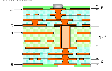
Substrate Layer Stackup
Package substrate hierarchy and PCB design
In PCB (Printed Circuit Board) design, the hierarchical structure of the packaging substrate plays a vital role, directly affecting the performance and complexity of electronic devices. The following is a detailed discussion of the close relationship between package substrate hierarchy and PCB design:
The hierarchical configuration of a packaging substrate significantly and directly influences the performance of the PCB (Printed Circuit Board). Comprising the top layer (surface layer), inner layer (inner layer), and bottom layer (bottom layer), each segment serves distinct functions that collaboratively form a cohesive system. The top layer typically accommodates component placement, the inner layer houses intricate signal layers, and the bottom layer assumes responsibility for mechanical support and circuit connectivity. Through skillful design of the layout and connections within each layer, designers can achieve elevated circuit density and enhanced signal integrity, consequently augmenting overall performance.
When considering the packaging substrate hierarchy, designers need to make a series of critical decisions that directly impact the reliability and manufacturing cost of the electronic device. First, the designer needs to determine the number and layout of hierarchical structures to meet the functional requirements of the circuit. Multilayer structures provide greater design freedom, but also increase manufacturing and troubleshooting complexity.
Second, determining the materials and thickness of each layer in the hierarchy is critical for electromagnetic compatibility and thermal performance. Reasonable selection of materials can effectively reduce signal interference and ensure the stability of electronic equipment in different working environments.
Additionally, designers need to evaluate the maintainability and upgradeability of the hierarchy, taking into account future maintenance and upgrade needs. Good design not only considers current technical needs, but also has a long-term vision to adapt to the rapid development of the electronic field in the future.
Overall, the design of hierarchical structure is a key link in PCB design, which requires comprehensive consideration of performance, complexity, materials, and future maintainability. Reasonable decisions will directly determine the performance level and market competitiveness of electronic equipment.
This also demonstrates the core position of the packaging substrate hierarchy in the modern electronics industry and is critical to driving progress in the electronics field. Through innovative and sustainable practices, designers will continue to challenge and push technological boundaries, laying a solid foundation for the future development of the electronics industry.
Advantages of Package Substrate Hierarchy
The hierarchical structure of packaging substrates plays a vital role in modern electronic design. Its multi-layer design not only provides higher density for circuits, but also brings excellent performance and flexibility. At this level, we will delve into the advantages of multi-layered structures and emphasize the indispensability of the layers working together.
Higher density and compactness
The multi-layer structure of the packaging substrate allows circuit components to be laid out in a smaller space, thereby achieving higher component density. This increase in density is particularly critical for modern electronic devices because it allows more functions and performance to be integrated into a relatively small space, making the device possible for compact design.
By arranging circuit components on different levels, designers can utilize space vertically instead of just horizontally. This vertical integration method allows the circuit board to accommodate more functional components, thereby promoting the reduction of device size and improvement of functional performance.
Emphasis on the importance of collaborative work among all layers
One of the advantages of multilayer packaging substrates is how the layers work together. Different levels of circuit components and signal layers can interact more effectively, enabling more complex and sophisticated circuit designs. This collaborative effort not only improves the performance of the circuit, it also helps reduce the overall complexity of the board.
Multilayer packaging substrates offer a distinct advantage through the synergistic interaction of their layers. This collaborative approach facilitates more effective interactions between different levels of circuit components and signal layers, paving the way for intricate and sophisticated circuit designs. This not only enhances circuit performance but also streamlines the overall complexity of the board.
The synergy among layers contributes to shorter signal transmission paths, minimizing signal transmission delays, and bolstering the system’s response speed. Simultaneously, it mitigates electromagnetic interference (EMI) and crosstalk, thereby improving overall signal integrity.
The multilayer structure of packaging substrates emerges as a compelling asset in electronic device design, enabling heightened density and performance. Its collaborative design characteristics bring different levels of the design closer, establishing a robust foundation for ongoing innovation and sustainable development within the electronics industry. Looking ahead, as technology continues its evolution, the multi-layered design of packaging substrates is poised to remain at the forefront of innovation trends in the electronics sector.