 Professional Flip-Chip Packaging Substrate Supplier

Ultra-Multilayer FC-BGA Package Substrates Manufacturer.”Ultra-Multilayer FC-BGA Package Substrates Manufacturer” refers to a company specializing in the production of complex, multi-layered substrates for FC-BGA packaging. They excel in crafting advanced interconnect solutions that enhance performance and reliability in electronic devices.
What are Ultra-Multilayer FC-BGA Package Substrates?
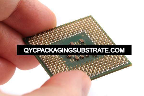
Ultra-Multilayer FC-BGA Package Substrates, namely ultra-multilayer FC-BGA package substrates, are a vital component in modern electronic equipment. They are usually flat plates made of insulating materials such as FR4, with various electronic components such as integrated circuit chips, resistors and capacitors mounted on the surface. These components are connected and interconnected through a complex copper layer structure on the substrate.
In Ultra-Multilayer FC-BGA Package Substrates, the copper layer not only provides a transmission path for electronic signals, but also forms the pads and other necessary connection features. These pads are used to secure and connect electronic components, ensuring they work securely in the circuit. The design and manufacturing accuracy of the substrate are crucial to the performance and reliability of the device, so Ultra-Multilayer FC-BGA Package Substrates usually adopt high-precision manufacturing processes and advanced technologies.
As modern electronic devices have increasingly higher requirements for performance and size, Ultra-Multilayer FC-BGA Package Substrates are widely used due to their compact design and excellent electrical performance. They enable the layout of complex circuits in limited space and support high-speed data transmission and signal processing requirements. In addition to regular fixed functions, Ultra-Multilayer FC-BGA Package Substrates in certain applications also have high-frequency characteristics and thermal management capabilities, making them widely used in communications, computers, medical equipment and other fields.
Ultra-Multilayer FC-BGA Package Substrates Manufacturer
In short, Ultra-Multilayer FC-BGA Package Substrates, as an indispensable part of modern electronic technology, provide key support for the functionality, performance and reliability of various electronic devices through its complex and precise design and manufacturing process. Promoted the development and innovation of the entire industry.
Ultra-Multilayer FC-BGA Package Substrates design Reference Guide.
The Ultra-Multilayer FC-BGA Package Substrates Design Reference Guide is an important tool for electronic engineers and designers when developing and optimizing substrate layouts. This comprehensive handbook covers many aspects to ensure efficient and reliable substrate design.
First, the Design Reference Guide emphasizes the importance of best practices. By following industry-recognized best practices, engineers can reduce potential design issues and manufacturing defects, saving time and money. This includes comprehensive guidance from layout design to electrical characteristic analysis to ensure that the design meets functional requirements while having good electrical performance and thermal management capabilities.
Second, design rules feature prominently in the guidelines. These rules cover recommended values and constraints for key parameters such as routing, spacing, apertures, impedance control, and more. By adhering to these rules, designers can minimize signal integrity issues and EMI (electromagnetic interference), ensuring reliable operation of the substrate in a variety of environmental conditions.
Software tools are another key component in a design reference guide. Modern design software not only enables complex layout and routing, but also performs electromagnetic field simulation, thermal analysis and 3D model generation to evaluate the feasibility of the design in terms of physical space and functional performance. The guide details the advantages and disadvantages of various software tools and their application recommendations at different stages.
Finally, design technology is one of the core contents of the guide. This includes technical guidance from multi-layer layout strategies to high-density component placement, as well as best practices for high-speed signal transmission and power distribution. The design technology section also discusses advanced packaging technologies and manufacturing processes, such as specific optimization solutions and implementation methods for ultra-multilayer FC-BGA packaging substrates.
To sum up, the Ultra-Multilayer FC-BGA Package Substrates Design Reference Guide is not only a technical manual, but also an important companion for engineers when facing complex design challenges. By following the guiding principles and practical advice in the guide, design teams can efficiently innovate and optimize during the design cycle to deliver high-performance, reliable electronic products to the market.
What material is used in Ultra-Multilayer FC-BGA Package Substrates?
Ultra-Multilayer FC-BGA Package Substrates (Ultra-Multilayer FC-BGA Package Substrates) are key components in modern electronic equipment, and their material selection is crucial, directly affecting their performance and applicability. Normally, Ultra-Multilayer FC-BGA Package Substrates mainly uses FR4 (fiberglass reinforced epoxy resin laminate) as the base material. FR4 material has excellent electrical insulation properties and mechanical strength, making it one of the preferred materials widely used in PCB manufacturing.
The advantages of FR4 materials include its stability in high-frequency and high-temperature environments, as well as good machining properties, which can meet the needs of complex circuit layouts. Its thermal and chemical resistance allows Ultra-Multilayer FC-BGA Package Substrates to maintain stability and reliability under extreme conditions.
In addition to FR4, some application scenarios may also require the use of flexible base materials such as polyimide (PI). Polyimide’s excellent flexibility and high-temperature stability make it suitable for applications that require bending and folding, such as flexible electronics or space-constrained device layouts.
During the design and manufacturing process of Ultra-Multilayer FC-BGA Package Substrates, materials are selected not only based on their physical and chemical properties, but also on cost-effectiveness and production feasibility. Therefore, when engineers and designers formulate substrate design plans, they usually carefully select the most appropriate materials based on the requirements of the specific application to ensure that the final product achieves the best balance between performance, reliability, and cost.
In short, the material selection of Ultra-Multilayer FC-BGA Package Substrates is one of the key factors for its successful application in various fields. As technology continues to advance and market demands change, the exploration of new materials and technologies will continue to drive the development and innovation of these key components.
What size are Ultra-Multilayer FC-BGA Package Substrates?
The size of Ultra-Multilayer FC-BGA Package Substrates plays a crucial role in the design of electronic devices because of its wide adaptability, covering everything from micro to large substrates. The size of these substrates depends on the specific application needs and the design and functional requirements of the device.
Driven by the development of modern technology, Ultra-Multilayer FC-BGA Package Substrates are widely used in various devices, including smartphones, wearable devices, industrial equipment, and power electronics. For example, in smartphones and wearable devices, substrates are often designed to be tiny and compact to accommodate the trend of device miniaturization. This tiny size requires the substrate to accommodate a variety of complex electronic components and achieve efficient circuit connections and signal transmission within a limited space to ensure device performance and reliability.
In contrast, Ultra-Multilayer FC-BGA Package Substrates for industrial equipment or power electronics generally require larger size and higher power carrying capabilities. These large substrates are able to accommodate more electronic components and connectors and handle more complex circuit design and power management needs. Its design takes into account the space layout and heat dissipation requirements inside the device to ensure stable performance under harsh environmental conditions such as high pressure and high temperature.
Overall, the size of Ultra-Multilayer FC-BGA Package Substrates is not only determined by the size and complexity of the electronic components themselves, but also by the available space and functional requirements inside the device. Through precise dimensional design and optimization, these substrates enable optimal circuit layout and signal transmission efficiency, providing a solid foundation for the functionality and performance of modern electronic devices.
Therefore, understanding and rationally selecting the size of Ultra-Multilayer FC-BGA Package Substrates is crucial to ensuring that the overall design and functionality of the device are optimal. This is also an important direction for electronic engineers and designers to continue to explore and optimize in their work. one.
The Manufacturer Process of Ultra-Multilayer FC-BGA Package Substrates.
The manufacturing process of Ultra-Multilayer FC-BGA Package Substrates is a precise and complex process involving multiple key steps. Each step is crucial and directly affects the quality and quality of the final product. performance.
First, the manufacturing process begins with the substrate preparation stage. At this stage, it is critical to select the appropriate substrate material, usually FR4 (fiberglass reinforced epoxy laminate) is used, which is widely favored for its excellent electrical properties and mechanical strength. Substrate preparation also includes treating the surface to ensure it is suitable for subsequent copper layer deposition and patterning.
Next comes the deposition of the copper layer. The copper layer is chemically deposited evenly on the substrate surface to form conductive paths and pad areas. The accuracy of this step is critical to the conductivity and stability of the final circuit board.
Photoresist application and exposure are the next critical steps. At this stage, photoresist is coated on the copper layer and then exposed to form the desired circuit pattern using a mask and UV light. After exposure, the unexposed photoresist is removed, exposing areas of the copper layer that need to be etched.
Etching is one of the important steps in the manufacturing process. The area of the copper layer that is not protected by the photoresist is etched away through a chemical solution to form the wires and pads of the circuit board. The precision and control of etching has a direct impact on the performance and reliability of the circuit board.
After etching is complete, the next step is drilling. According to the design requirements, drill holes at the predetermined locations to prepare the locations for the installation and welding of subsequent components. These holes may be for through-hole technology or they may be mounting pads for surface mount technology (SMT).
Component installation is another critical step in the manufacturing process. At this stage, electronic components are accurately placed on the circuit board according to the design layout, and automated precision assembly equipment can be used to ensure the correct position and positioning accuracy of each component.
Finally comes the welding and testing phase. Soldering connects electronic components to the pads on the circuit board by heating the solder to ensure smoothness and stability of the circuit. After completing the welding, strict functional testing and electrical performance testing are performed to ensure that the circuit board meets the design requirements and quality standards.
In summary, the manufacturing process of Ultra-Multilayer FC-BGA Package Substrates combines advanced materials science and precision manufacturing technology. Through careful design and strict control of each step, we ensure that the final circuit board reaches the best level of performance, reliability and cost-effectiveness to meet the needs of modern high-tech applications.
The Application area of Ultra-Multilayer FC-BGA Package Substrates.
Ultra-Multilayer FC-BGA Package Substrates (Ultra-Multilayer FC-BGA Package Substrates) are indispensable key components in modern electronic equipment. Its applications widely cover consumer electronics, communications, automobiles, aerospace, medical equipment, and industrial automation. multiple important industries. The following are its main application areas in various industries:
In the field of consumer electronics, Ultra-Multilayer FC-BGA Package Substrates are widely used in products such as smartphones, tablets, portable entertainment devices and home appliances. These substrates not only support complex circuit connections and control of devices, but also enable miniaturized designs to meet consumer demands for portability and high performance.
In communication technology, Ultra-Multilayer FC-BGA Package Substrates are used in key facilities such as base station equipment, network routers, communication satellites and optical fiber communication equipment. They can provide highly stable signal transmission and processing capabilities and support complex data processing and communication protocols.
In automotive electronic systems, Ultra-Multilayer FC-BGA Package Substrates play an important role in connecting and controlling various automotive electronic devices, such as engine control units (ECUs), vehicle infotainment systems, airbag controllers, etc. They need to operate stably in harsh environmental conditions and withstand the effects of vibration and temperature changes.
In the aerospace field, Ultra-Multilayer FC-BGA Package Substrates are used in avionics equipment and satellite platforms, such as flight control systems, communication equipment, navigation systems and satellite payloads. They must have high reliability and radiation resistance to ensure long-term stable operation in extreme environments.
In the medical field, Ultra-Multilayer FC-BGA Package Substrates are used in various medical diagnostic equipment, patient monitoring systems and treatment equipment. They support precise data collection and processing, ensure the accuracy and reliability of medical equipment, and play a key role in medical treatment and diagnosis.
In industrial automation applications, Ultra-Multilayer FC-BGA Package Substrates are used in control systems, sensor networks, industrial robots and automated production lines. They can handle complex control logic and data exchange, improving production efficiency and the intelligence level of industrial equipment.
Overall, Ultra-Multilayer FC-BGA Package Substrates are not only basic components in modern electronic equipment, but also play a key role in promoting technological progress and innovation in various industries. Their application range covers a wide range of fields, from smartphones and computers to medical equipment and satellites, providing solid technical support for the functionality, performance and reliability of various types of equipment.
What are the advantages of Ultra-Multilayer FC-BGA Package Substrates?
Ultra-Multilayer FC-BGA Package Substrates have significant multiple advantages in the field of electronic engineering compared to other wiring methods. Below is a detailed description of its main advantages:
First, Ultra-Multilayer FC-BGA Package Substrates enable highly compact layouts, which enables electronic devices to be miniaturized in size. By utilizing multi-layer structure and advanced design technology, Ultra-Multilayer FC-BGA Package Substrates effectively integrates multiple electronic components in a relatively limited space, thereby significantly reducing the size of the device and adapting to the design needs of modern consumer electronics and portable devices. .
Secondly, Ultra-Multilayer FC-BGA Package Substrates adopt standardized manufacturing processes to ensure consistent quality and reliability. Through strict quality control and automated production technology, these substrates are able to maintain a high level of stability in mass production and reduce failure rates caused by manufacturing differences, thus improving the overall reliability and long-term stability of the equipment.
Third, Ultra-Multilayer FC-BGA Package Substrates show great convenience during the assembly process. The automated assembly process not only simplifies the production process, but also significantly reduces labor costs and time consumption. This efficient assembly method not only improves production efficiency, but also reduces the possibility of human error, ensuring product consistency and quality.
In addition, Ultra-Multilayer FC-BGA Package Substrates are highly customizable and can be flexibly designed according to specific application requirements. Whether it is complex circuit layout or the integration of multiple components, these substrates can meet engineers’ precise requirements for performance and functionality, providing tailor-made solutions for various application scenarios.
Finally, Ultra-Multilayer FC-BGA Package Substrates have clear economic advantages since mass production can significantly reduce the cost per unit substrate. This makes them particularly suitable for markets requiring high-volume manufacturing, such as consumer electronics and industrial automation. By reducing unit costs, manufacturers can increase product market competitiveness and profit margins while maintaining product quality and performance.
To sum up, Ultra-Multilayer FC-BGA Package Substrates has become an indispensable key technology in modern electronic design and manufacturing with its compact layout, reliable quality, convenient assembly, flexible customization and economical production cost. , promoting the continuous innovation and progress of electronic products.
FAQ
What are Ultra-Multilayer FC-BGA Package Substrates?
Ultra-Multilayer FC-BGA Package Substrates (Ultra-Multilayer FC-BGA Package Substrate) is a highly complex electronic packaging technology that interconnects electronic components and circuits through multi-level structures and BGA (Ball Grid Array) packaging technology. connected together. This packaging substrate not only provides excellent electrical performance and mechanical strength, but also supports high-density, high-speed circuit design.
What are the main advantages of Ultra-Multilayer FC-BGA Package Substrates?
Ultra-Multilayer FC-BGA Package Substrates have multiple advantages over traditional substrates. They enable compact circuit layouts and support the integration of complex circuits while providing highly reliable electrical connections and mechanical support. This packaging technology not only improves the performance and reliability of the device, but also can adapt to the needs of various application scenarios, including high-frequency, high-speed and high-density electronic equipment.
What is the manufacturing process of Ultra-Multilayer FC-BGA Package Substrates?
The manufacturing process of Ultra-Multilayer FC-BGA Package Substrates involves several key steps. The first is substrate preparation, including material selection and pretreatment. Then proceed to multi-layer stacking, deposition of copper foil layers, application and exposure of photoresist, etching to form circuit patterns, followed by drilling, surface treatment, and installation of BGA ball grid arrays. Finally, testing and quality control are performed to ensure that the performance of the packaging substrate meets the design requirements.