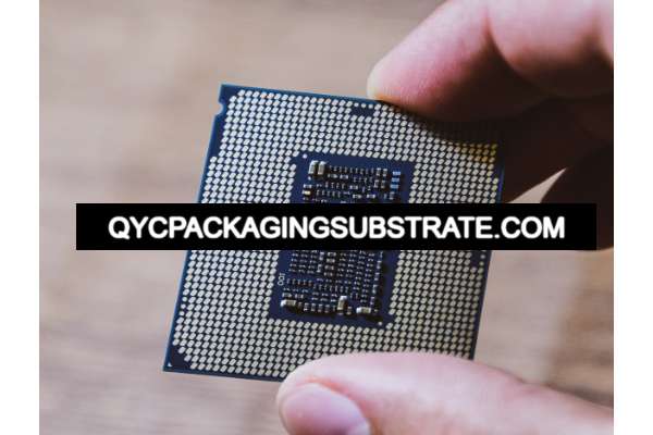
Ultra-Multilayer FCCSP Substrates Manufacturer.As a leading Ultra-Multilayer FCCSP Substrates Manufacturer, we specialize in producing high-performance substrates that support advanced semiconductor packaging. Our cutting-edge technology and rigorous quality control ensure optimal signal integrity, thermal management, and reliability for high-density electronic applications. Trust us to deliver innovative solutions that meet the demands of modern electronics.
Ultra-Multilayer FCCSP (Flip Chip Chip Scale Package) substrates are advanced packaging solutions designed for high-performance, high-density semiconductor applications. These substrates support complex interconnections and provide enhanced electrical, thermal, and mechanical properties. This article explores the properties, structure, materials, manufacturing processes, applications, advantages, and frequently asked questions (FAQs) related to Ultra-Multilayer FCCSP substrates.
Structure of Ultra-Multilayer FCCSP Substrates
The structure of Ultra-Multilayer FCCSP substrates is designed to support the demanding requirements of modern semiconductor devices:
The substrate is typically made from high-performance materials such as BT (Bismaleimide-Triazine) resin or ABF (Ajinomoto Build-up Film) to provide excellent mechanical strength, thermal stability, and electrical insulation.

Ultra-Multilayer FCCSP Substrates Manufacturer
Multiple layers of copper are used for the conductive traces. These layers are precisely patterned to form complex interconnections that connect the semiconductor die to the external circuitry.
High-performance dielectric materials are used between the conductive layers to provide electrical isolation and maintain signal integrity.
Through-holes and microvias are used to create vertical interconnections between the different layers of the substrate, enabling high-density routing.
A variety of surface finishes, such as ENIG (Electroless Nickel Immersion Gold) or OSP (Organic Solderability Preservatives), are applied to enhance solderability and protect the copper surfaces from oxidation.
Materials Used in Ultra-Multilayer FCCSP Substrates
Key materials used in Ultra-Multilayer FCCSP substrates include:
A high-performance thermosetting resin known for its excellent thermal and mechanical properties, making it suitable for high-reliability applications.
A type of epoxy resin film used for its excellent electrical insulation properties, high glass transition temperature, and good adhesion to copper.
High-purity copper is used for conductive traces due to its excellent electrical conductivity and reliability.
High-performance dielectric materials with low dielectric constant and low loss tangent are used to ensure minimal signal loss and distortion.
Surface finishes such as ENIG and OSP are applied to protect the copper traces and enhance solderability.
Manufacturing Process of Ultra-Multilayer FCCSP Substrates
The manufacturing process for Ultra-Multilayer FCCSP substrates involves several precise steps:
Selection of base materials and conductive layers based on performance requirements.
Stacking and bonding multiple layers of conductive and dielectric materials under controlled conditions to form a stable substrate.
Precision drilling and laser drilling are used to create through-holes and microvias for vertical interconnections between layers.
Electroplating copper onto the substrate and inside vias to establish reliable electrical connections.
Using photolithography and chemical etching to define the circuit patterns and interconnects.
Applying protective coatings to exposed copper surfaces to enhance solderability and protect against oxidation.
Attaching the semiconductor die and other components to the substrate using advanced soldering techniques, ensuring minimal signal loss and distortion.
Rigorous testing for electrical performance, signal integrity, and adherence to design specifications.
Applications of Ultra-Multilayer FCCSP Substrates
Ultra-Multilayer FCCSP substrates are used in a wide range of high-performance applications, including:
Smartphones, tablets, and wearable devices that require high-density packaging and high-speed signal transmission.
Base stations, network routers, and other communication infrastructure that demand high-performance and reliable interconnections.
Advanced driver-assistance systems (ADAS), infotainment systems, and other electronic components in vehicles.
High-performance computing and control systems used in manufacturing and process automation.
Diagnostic and imaging equipment that require high reliability and precision.
Advantages of Ultra-Multilayer FCCSP Substrates
Ultra-Multilayer FCCSP substrates offer several significant advantages:
The multilayer structure allows for complex and high-density routing, enabling advanced semiconductor designs.
Maintains high signal quality and integrity through the use of low-loss materials and precise manufacturing processes.
Effective heat dissipation through substrate materials and design features, ensuring stable operation under high-power conditions.
Robust construction and testing ensure long-term performance and reliability in demanding applications.
Suitable for a wide range of high-performance applications across various industries.
FAQ
What materials are typically used for Ultra-Multilayer FCCSP substrates, and why?
Ultra-Multilayer FCCSP substrates commonly use materials like BT resin and ABF for their excellent thermal stability, mechanical strength, and electrical insulation properties. These materials are essential for maintaining reliability and performance in high-density and high-speed applications.
How do Ultra-Multilayer FCCSP substrates differ from standard PCBs?
Ultra-Multilayer FCCSP substrates are designed specifically for high-performance semiconductor packaging, using advanced materials and manufacturing processes to support high-density interconnections and high-frequency signal transmission. Standard PCBs are typically used for less demanding applications and may not require such stringent performance characteristics.
What industries benefit the most from the use of Ultra-Multilayer FCCSP substrates?
Industries such as consumer electronics, telecommunications, automotive electronics, industrial automation, and medical devices benefit significantly from the use of Ultra-Multilayer FCCSP substrates due to their high-density interconnections, signal integrity, and reliability.
How are Ultra-Multilayer FCCSP substrates tested to ensure reliability?
Ultra-Multilayer FCCSP substrates undergo rigorous testing processes, including electrical testing for signal integrity and performance, thermal cycling, and reliability testing. These tests ensure that the substrates meet stringent performance and durability standards required for high-performance applications.
 Professional Flip-Chip Packaging Substrate Supplier
